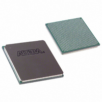
EP1S20F780I6N Altera, EP1S20F780I6N Datasheet - Page 626

EP1S20F780I6N
Manufacturer Part Number
EP1S20F780I6N
Description
IC STRATIX FPGA 20K LE 780-FBGA
Manufacturer
Altera
Series
Stratix®r
Specifications of EP1S20F780I6N
Number Of Logic Elements/cells
18460
Number Of Labs/clbs
1846
Total Ram Bits
1669248
Number Of I /o
586
Voltage - Supply
1.425 V ~ 1.575 V
Mounting Type
Surface Mount
Operating Temperature
-40°C ~ 100°C
Package / Case
780-FBGA
Family Name
Stratix
Number Of Logic Blocks/elements
18460
# I/os (max)
586
Frequency (max)
450.05MHz
Process Technology
0.13um (CMOS)
Operating Supply Voltage (typ)
1.5V
Logic Cells
18460
Ram Bits
1669248
Operating Supply Voltage (min)
1.425V
Operating Supply Voltage (max)
1.575V
Operating Temp Range
-40C to 100C
Operating Temperature Classification
Industrial
Mounting
Surface Mount
Pin Count
780
Package Type
FC-FBGA
Lead Free Status / RoHS Status
Lead free / RoHS Compliant
Number Of Gates
-
Lead Free Status / Rohs Status
Compliant
Available stocks
Company
Part Number
Manufacturer
Quantity
Price
Company:
Part Number:
EP1S20F780I6N
Manufacturer:
ALTERA
Quantity:
3 000
- Current page: 626 of 864
- Download datasheet (11Mb)
Matrix Manipulation
Figure 7–27. Using Free Boundary Condition for Edge Pixels
7–48
Stratix Device Handbook, Volume 2
Image boundary
0
0
0
3 x 3 kernel slides across image
x( x x m + 1, n )
x( x x
black pixels, that is pixels with value zero. This is similar to padding the
edges of the input image matrix with zeros and is referred to as the free
boundary condition. This is shown in
Convolution Implementation
This design example shows a 3
input image with gray pixel values ranging from 0-255 (8-bit). Data is fed
in serially starting from the top left pixel, moving horizontally on a row-
by-row basis. Next the data is stored in three separate RAM blocks in the
buffering stage. Each M512 memory block represents a line of the image,
and this is cycled through. For a 32
M4K memory blocks. For larger images (640
to M-RAM blocks or other buffering schemes. The control logic block
provides the RAM control signals to interleave the data across all three
0
x( x x m + 1, n + 1)
x( x x m , n + 1)
0
3 2-D FIR filter that takes in an 8
32 input image, the design needs
Figure
7–27.
480), this can be extended
Image boundary
Altera Corporation
Image
September 2004
8
Related parts for EP1S20F780I6N
Image
Part Number
Description
Manufacturer
Datasheet
Request
R

Part Number:
Description:
CYCLONE II STARTER KIT EP2C20N
Manufacturer:
Altera
Datasheet:

Part Number:
Description:
CPLD, EP610 Family, ECMOS Process, 300 Gates, 16 Macro Cells, 16 Reg., 16 User I/Os, 5V Supply, 35 Speed Grade, 24DIP
Manufacturer:
Altera Corporation
Datasheet:

Part Number:
Description:
CPLD, EP610 Family, ECMOS Process, 300 Gates, 16 Macro Cells, 16 Reg., 16 User I/Os, 5V Supply, 15 Speed Grade, 24DIP
Manufacturer:
Altera Corporation
Datasheet:

Part Number:
Description:
Manufacturer:
Altera Corporation
Datasheet:

Part Number:
Description:
CPLD, EP610 Family, ECMOS Process, 300 Gates, 16 Macro Cells, 16 Reg., 16 User I/Os, 5V Supply, 30 Speed Grade, 24DIP
Manufacturer:
Altera Corporation
Datasheet:

Part Number:
Description:
High-performance, low-power erasable programmable logic devices with 8 macrocells, 10ns
Manufacturer:
Altera Corporation
Datasheet:

Part Number:
Description:
High-performance, low-power erasable programmable logic devices with 8 macrocells, 7ns
Manufacturer:
Altera Corporation
Datasheet:

Part Number:
Description:
Classic EPLD
Manufacturer:
Altera Corporation
Datasheet:

Part Number:
Description:
High-performance, low-power erasable programmable logic devices with 8 macrocells, 10ns
Manufacturer:
Altera Corporation
Datasheet:

Part Number:
Description:
Manufacturer:
Altera Corporation
Datasheet:

Part Number:
Description:
Manufacturer:
Altera Corporation
Datasheet:

Part Number:
Description:
Manufacturer:
Altera Corporation
Datasheet:

Part Number:
Description:
CPLD, EP610 Family, ECMOS Process, 300 Gates, 16 Macro Cells, 16 Reg., 16 User I/Os, 5V Supply, 25 Speed Grade, 24DIP
Manufacturer:
Altera Corporation
Datasheet:


