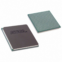
EP1S20F780I6N Altera, EP1S20F780I6N Datasheet - Page 408

EP1S20F780I6N
Manufacturer Part Number
EP1S20F780I6N
Description
IC STRATIX FPGA 20K LE 780-FBGA
Manufacturer
Altera
Series
Stratix®r
Specifications of EP1S20F780I6N
Number Of Logic Elements/cells
18460
Number Of Labs/clbs
1846
Total Ram Bits
1669248
Number Of I /o
586
Voltage - Supply
1.425 V ~ 1.575 V
Mounting Type
Surface Mount
Operating Temperature
-40°C ~ 100°C
Package / Case
780-FBGA
Family Name
Stratix
Number Of Logic Blocks/elements
18460
# I/os (max)
586
Frequency (max)
450.05MHz
Process Technology
0.13um (CMOS)
Operating Supply Voltage (typ)
1.5V
Logic Cells
18460
Ram Bits
1669248
Operating Supply Voltage (min)
1.425V
Operating Supply Voltage (max)
1.575V
Operating Temp Range
-40C to 100C
Operating Temperature Classification
Industrial
Mounting
Surface Mount
Pin Count
780
Package Type
FC-FBGA
Lead Free Status / RoHS Status
Lead free / RoHS Compliant
Number Of Gates
-
Lead Free Status / Rohs Status
Compliant
Available stocks
Company
Part Number
Manufacturer
Quantity
Price
Company:
Part Number:
EP1S20F780I6N
Manufacturer:
ALTERA
Quantity:
3 000
- Current page: 408 of 864
- Download datasheet (11Mb)
DDR Memory Support Overview
3–12
Stratix Device Handbook, Volume 2
Figure 3–7
Figure 3–7. Stratix & Stratix GX Device DQ & DQS Groups in × 8 Mode
Note to
(1)
Data & Data Strobe Pins
Stratix and Stratix GX data pins for the DDR memory interfaces are called
DQ pins. The Stratix and Stratix GX device I/O banks at the top (I/O
banks 3 and 4) and the bottom (I/O banks 7 and 8) of the device support
DDR SDRAM and RLDRAM II up to 200 MHz. These pins support DQS
signals with DQ bus modes of ×8, ×16, or ×32. Stratix and Stratix GX
devices can support either bidirectional data strobes or uni-directional
read clocks. Depending on the external memory interface, either the
memory device's read data strobes or read clocks feed the DQS pins.
For ×8 mode, there are up to 20 groups of programmable DQS and DQ
pins—10 groups in I/O banks 3 and 4 and 10 groups in I/O banks 7 and 8
(see
pins.
For ×16 mode, there are up to eight groups of programmable DQS and
DQ pins—four groups in I/O banks 3 and 4, and four groups in I/O
banks 7 and 8. The EP1S20 device supports seven ×16 mode groups. The
EP1S10 device does not support ×16 mode. All other devices support the
full eight groups. See
DQ pins. In ×16 mode, DQS1T, DQS3T, DQS6T, and DQS8T pins on the top
side of the device, and DQS1B, DQS3B, DQS6B, and DQS8B pins on the
Top or Bottom I/O Bank
Table
There are at least eight DQ pins per group.
Figure
3–3). Each group consists of one DQS pin and a set of eight DQ
shows the DQ and DQS pins in ×8 mode.
3–7:
DQ Pins (1)
Table
3–3. Each group consists of one DQS and 16
DQS Pin
Altera Corporation
June 2006
Related parts for EP1S20F780I6N
Image
Part Number
Description
Manufacturer
Datasheet
Request
R

Part Number:
Description:
CYCLONE II STARTER KIT EP2C20N
Manufacturer:
Altera
Datasheet:

Part Number:
Description:
CPLD, EP610 Family, ECMOS Process, 300 Gates, 16 Macro Cells, 16 Reg., 16 User I/Os, 5V Supply, 35 Speed Grade, 24DIP
Manufacturer:
Altera Corporation
Datasheet:

Part Number:
Description:
CPLD, EP610 Family, ECMOS Process, 300 Gates, 16 Macro Cells, 16 Reg., 16 User I/Os, 5V Supply, 15 Speed Grade, 24DIP
Manufacturer:
Altera Corporation
Datasheet:

Part Number:
Description:
Manufacturer:
Altera Corporation
Datasheet:

Part Number:
Description:
CPLD, EP610 Family, ECMOS Process, 300 Gates, 16 Macro Cells, 16 Reg., 16 User I/Os, 5V Supply, 30 Speed Grade, 24DIP
Manufacturer:
Altera Corporation
Datasheet:

Part Number:
Description:
High-performance, low-power erasable programmable logic devices with 8 macrocells, 10ns
Manufacturer:
Altera Corporation
Datasheet:

Part Number:
Description:
High-performance, low-power erasable programmable logic devices with 8 macrocells, 7ns
Manufacturer:
Altera Corporation
Datasheet:

Part Number:
Description:
Classic EPLD
Manufacturer:
Altera Corporation
Datasheet:

Part Number:
Description:
High-performance, low-power erasable programmable logic devices with 8 macrocells, 10ns
Manufacturer:
Altera Corporation
Datasheet:

Part Number:
Description:
Manufacturer:
Altera Corporation
Datasheet:

Part Number:
Description:
Manufacturer:
Altera Corporation
Datasheet:

Part Number:
Description:
Manufacturer:
Altera Corporation
Datasheet:

Part Number:
Description:
CPLD, EP610 Family, ECMOS Process, 300 Gates, 16 Macro Cells, 16 Reg., 16 User I/Os, 5V Supply, 25 Speed Grade, 24DIP
Manufacturer:
Altera Corporation
Datasheet:


