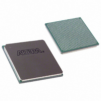
EP1S20F780I6N Altera, EP1S20F780I6N Datasheet - Page 421

EP1S20F780I6N
Manufacturer Part Number
EP1S20F780I6N
Description
IC STRATIX FPGA 20K LE 780-FBGA
Manufacturer
Altera
Series
Stratix®r
Specifications of EP1S20F780I6N
Number Of Logic Elements/cells
18460
Number Of Labs/clbs
1846
Total Ram Bits
1669248
Number Of I /o
586
Voltage - Supply
1.425 V ~ 1.575 V
Mounting Type
Surface Mount
Operating Temperature
-40°C ~ 100°C
Package / Case
780-FBGA
Family Name
Stratix
Number Of Logic Blocks/elements
18460
# I/os (max)
586
Frequency (max)
450.05MHz
Process Technology
0.13um (CMOS)
Operating Supply Voltage (typ)
1.5V
Logic Cells
18460
Ram Bits
1669248
Operating Supply Voltage (min)
1.425V
Operating Supply Voltage (max)
1.575V
Operating Temp Range
-40C to 100C
Operating Temperature Classification
Industrial
Mounting
Surface Mount
Pin Count
780
Package Type
FC-FBGA
Lead Free Status / RoHS Status
Lead free / RoHS Compliant
Number Of Gates
-
Lead Free Status / Rohs Status
Compliant
Available stocks
Company
Part Number
Manufacturer
Quantity
Price
Company:
Part Number:
EP1S20F780I6N
Manufacturer:
ALTERA
Quantity:
3 000
- Current page: 421 of 864
- Download datasheet (11Mb)
Altera Corporation
June 2006
The Stratix and Stratix GX DDR IOE structure requires you to invert the
incoming DQS signal by using a NOT gate to ensure proper data transfer.
The altdq megafunction automatically adds the inverter when it
generates the DQ signals. As shown in
rising edge clocks the A
the B
memory read operation, the last data coincides with DQS being low. If
you do not invert the DQS pin, you do not get this last data because the
latch does not open until the next rising edge of the DQS signal. The NOT
gate is inserted automatically if the altdg megafunction is used;
otherwise you need to add the NOT gate manually.
Figure 3–14
second set of waveforms in
shifted DQS signal is not inverted; the last data, D
into the logic array as DQS goes to tristate after the read postamble time.
The third set of waveforms in
with the DQS signal inverted after the 90° shift; the last data D
latched. In this case the outputs of register A
correspond to dataout_h and dataout_l ports, are now switched
because of the DQS inversion.
I
register, and latch C
shows waveforms of the circuit shown in
External Memory Interfaces in Stratix & Stratix GX Devices
I
register, inclock signal's falling edge clocks
I
is opened when inclock is one. In a DDR
Figure 3–14
Figure 3–14
Figure
Stratix Device Handbook, Volume 2
shows what happens if the
shows a proper read operation
I
3–10, the inclock signal's
and latch C
n
, does not get latched
Figure
I
, which
3–12. The
n
does get
3–25
Related parts for EP1S20F780I6N
Image
Part Number
Description
Manufacturer
Datasheet
Request
R

Part Number:
Description:
CYCLONE II STARTER KIT EP2C20N
Manufacturer:
Altera
Datasheet:

Part Number:
Description:
CPLD, EP610 Family, ECMOS Process, 300 Gates, 16 Macro Cells, 16 Reg., 16 User I/Os, 5V Supply, 35 Speed Grade, 24DIP
Manufacturer:
Altera Corporation
Datasheet:

Part Number:
Description:
CPLD, EP610 Family, ECMOS Process, 300 Gates, 16 Macro Cells, 16 Reg., 16 User I/Os, 5V Supply, 15 Speed Grade, 24DIP
Manufacturer:
Altera Corporation
Datasheet:

Part Number:
Description:
Manufacturer:
Altera Corporation
Datasheet:

Part Number:
Description:
CPLD, EP610 Family, ECMOS Process, 300 Gates, 16 Macro Cells, 16 Reg., 16 User I/Os, 5V Supply, 30 Speed Grade, 24DIP
Manufacturer:
Altera Corporation
Datasheet:

Part Number:
Description:
High-performance, low-power erasable programmable logic devices with 8 macrocells, 10ns
Manufacturer:
Altera Corporation
Datasheet:

Part Number:
Description:
High-performance, low-power erasable programmable logic devices with 8 macrocells, 7ns
Manufacturer:
Altera Corporation
Datasheet:

Part Number:
Description:
Classic EPLD
Manufacturer:
Altera Corporation
Datasheet:

Part Number:
Description:
High-performance, low-power erasable programmable logic devices with 8 macrocells, 10ns
Manufacturer:
Altera Corporation
Datasheet:

Part Number:
Description:
Manufacturer:
Altera Corporation
Datasheet:

Part Number:
Description:
Manufacturer:
Altera Corporation
Datasheet:

Part Number:
Description:
Manufacturer:
Altera Corporation
Datasheet:

Part Number:
Description:
CPLD, EP610 Family, ECMOS Process, 300 Gates, 16 Macro Cells, 16 Reg., 16 User I/Os, 5V Supply, 25 Speed Grade, 24DIP
Manufacturer:
Altera Corporation
Datasheet:


