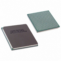
EP1S20F780I6N Altera, EP1S20F780I6N Datasheet - Page 753

EP1S20F780I6N
Manufacturer Part Number
EP1S20F780I6N
Description
IC STRATIX FPGA 20K LE 780-FBGA
Manufacturer
Altera
Series
Stratix®r
Specifications of EP1S20F780I6N
Number Of Logic Elements/cells
18460
Number Of Labs/clbs
1846
Total Ram Bits
1669248
Number Of I /o
586
Voltage - Supply
1.425 V ~ 1.575 V
Mounting Type
Surface Mount
Operating Temperature
-40°C ~ 100°C
Package / Case
780-FBGA
Family Name
Stratix
Number Of Logic Blocks/elements
18460
# I/os (max)
586
Frequency (max)
450.05MHz
Process Technology
0.13um (CMOS)
Operating Supply Voltage (typ)
1.5V
Logic Cells
18460
Ram Bits
1669248
Operating Supply Voltage (min)
1.425V
Operating Supply Voltage (max)
1.575V
Operating Temp Range
-40C to 100C
Operating Temperature Classification
Industrial
Mounting
Surface Mount
Pin Count
780
Package Type
FC-FBGA
Lead Free Status / RoHS Status
Lead free / RoHS Compliant
Number Of Gates
-
Lead Free Status / Rohs Status
Compliant
Available stocks
Company
Part Number
Manufacturer
Quantity
Price
Company:
Part Number:
EP1S20F780I6N
Manufacturer:
ALTERA
Quantity:
3 000
- Current page: 753 of 864
- Download datasheet (11Mb)
Figure 11–19. PPA Timing Waveforms Using Strobed nRS & nWS Signals
Notes to
(1)
(2)
(3)
(4)
Altera Corporation
July 2005
The user can toggle nCS or CS during configuration if the design meets the specification for t
Device I/O pins are in user mode.
The DATA[7..0] pins are available as user I/Os after configuration and the state of theses pins depends on the
dual-purpose pin settings. Do not leave DATA[7..0] floating. If these pins are not used in user-mode, you should
drive them high or low, whichever is more convenient.
DATA7 is a bidirectional pin. It represents an input for data input, but represents an output to show the status of
RDYnBSY.
DATA7/RDYnBSY (4)
Figure
CONF_DONE
11–19:
INIT_DONE
DATA[7..0]
nCONFIG
nSTATUS
User I/O
nCS (1)
CS (1)
nWS
nRS
t
CF2SCD
Figure 11–19
using strobed nRS and nWS signals.
t
CFG
t
WSP
t
WS2RS
t
CF2WS
t
CF2ST0
t
t
STATUS
t
CF2ST1
t
RDY2WS
RSD7
Byte 0
shows the Stratix and Stratix GX timing waveforms when
t
DSU
t
CSH
t
DH
Byte 1
t
RS2WS
t
t
CSSU
WS2RS
Configuring Stratix & Stratix GX Devices
t
WS2B
t
BUSY
Byte n
Stratix Device Handbook, Volume 2
CSSU
t
CD2UM
, t
(3)
(2)
(2)
(2)
(2)
(2)
(2)
WSP
, and t
11–35
CSH
.
Related parts for EP1S20F780I6N
Image
Part Number
Description
Manufacturer
Datasheet
Request
R

Part Number:
Description:
CYCLONE II STARTER KIT EP2C20N
Manufacturer:
Altera
Datasheet:

Part Number:
Description:
CPLD, EP610 Family, ECMOS Process, 300 Gates, 16 Macro Cells, 16 Reg., 16 User I/Os, 5V Supply, 35 Speed Grade, 24DIP
Manufacturer:
Altera Corporation
Datasheet:

Part Number:
Description:
CPLD, EP610 Family, ECMOS Process, 300 Gates, 16 Macro Cells, 16 Reg., 16 User I/Os, 5V Supply, 15 Speed Grade, 24DIP
Manufacturer:
Altera Corporation
Datasheet:

Part Number:
Description:
Manufacturer:
Altera Corporation
Datasheet:

Part Number:
Description:
CPLD, EP610 Family, ECMOS Process, 300 Gates, 16 Macro Cells, 16 Reg., 16 User I/Os, 5V Supply, 30 Speed Grade, 24DIP
Manufacturer:
Altera Corporation
Datasheet:

Part Number:
Description:
High-performance, low-power erasable programmable logic devices with 8 macrocells, 10ns
Manufacturer:
Altera Corporation
Datasheet:

Part Number:
Description:
High-performance, low-power erasable programmable logic devices with 8 macrocells, 7ns
Manufacturer:
Altera Corporation
Datasheet:

Part Number:
Description:
Classic EPLD
Manufacturer:
Altera Corporation
Datasheet:

Part Number:
Description:
High-performance, low-power erasable programmable logic devices with 8 macrocells, 10ns
Manufacturer:
Altera Corporation
Datasheet:

Part Number:
Description:
Manufacturer:
Altera Corporation
Datasheet:

Part Number:
Description:
Manufacturer:
Altera Corporation
Datasheet:

Part Number:
Description:
Manufacturer:
Altera Corporation
Datasheet:

Part Number:
Description:
CPLD, EP610 Family, ECMOS Process, 300 Gates, 16 Macro Cells, 16 Reg., 16 User I/Os, 5V Supply, 25 Speed Grade, 24DIP
Manufacturer:
Altera Corporation
Datasheet:


