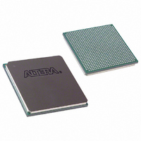
EP1S20F780I6N Altera, EP1S20F780I6N Datasheet - Page 778

EP1S20F780I6N
Manufacturer Part Number
EP1S20F780I6N
Description
IC STRATIX FPGA 20K LE 780-FBGA
Manufacturer
Altera
Series
Stratix®r
Specifications of EP1S20F780I6N
Number Of Logic Elements/cells
18460
Number Of Labs/clbs
1846
Total Ram Bits
1669248
Number Of I /o
586
Voltage - Supply
1.425 V ~ 1.575 V
Mounting Type
Surface Mount
Operating Temperature
-40°C ~ 100°C
Package / Case
780-FBGA
Family Name
Stratix
Number Of Logic Blocks/elements
18460
# I/os (max)
586
Frequency (max)
450.05MHz
Process Technology
0.13um (CMOS)
Operating Supply Voltage (typ)
1.5V
Logic Cells
18460
Ram Bits
1669248
Operating Supply Voltage (min)
1.425V
Operating Supply Voltage (max)
1.575V
Operating Temp Range
-40C to 100C
Operating Temperature Classification
Industrial
Mounting
Surface Mount
Pin Count
780
Package Type
FC-FBGA
Lead Free Status / RoHS Status
Lead free / RoHS Compliant
Number Of Gates
-
Lead Free Status / Rohs Status
Compliant
Available stocks
Company
Part Number
Manufacturer
Quantity
Price
Company:
Part Number:
EP1S20F780I6N
Manufacturer:
ALTERA
Quantity:
3 000
- Current page: 778 of 864
- Download datasheet (11Mb)
Device Configuration Pins
11–60
Stratix Device Handbook, Volume 2
TDI
TDO
TMS
TCK
TRST
Table 11–17. Dedicated JTAG pins
Pin Name
N/A
N/A
N/A
N/A
N/A
User Mode
Table 11–17
stable before and during configuration to prevent accidental loading of
JTAG instructions. If you plan to use the SignalTap II Embedded Logic
Analyzer, you will need to connect the JTAG pins of your device to a
JTAG header on your board.
Input
Output
Input
Input
Input
Pin Type
describes the dedicated JTAG pins. JTAG pins must be kept
Serial input pin for instructions as well as test and
programming data. Data is shifted in on the rising edge of
TCK
JTAG circuitry can be disabled by connecting this pin to
V
Serial data output pin for instructions as well as test and
programming data. Data is shifted out on the falling edge
of
of the device. If the JTAG interface is not required on the
board, the JTAG circuitry can be disabled by leaving this
pin unconnected.
Input pin that provides the control signal to determine the
transitions of the TAP controller state machine. Transitions
within the state machine occur on the rising edge of
Therefore,
TCK
JTAG interface is not required on the board, the JTAG
circuitry can be disabled by connecting this pin to V
This pin uses Schmitt trigger input buffers.
The clock input to the BST circuitry. Some operations
occur at the rising edge, while others occur at the falling
edge. If the JTAG interface is not required on the board, the
JTAG circuitry can be disabled by connecting this pin to
GND. This pin uses Schmitt trigger input buffers.
Active-low input to asynchronously reset the boundary-
scan circuit. The
Std. 1149.1. If the JTAG interface is not required on the
board, the JTAG circuitry can be disabled by connecting
this pin to GND. This pin uses Schmitt trigger input buffers.
C C
TCK
. This pin uses Schmitt trigger input buffers.
. If the JTAG interface is not required on the board, the
.
TMS
. The pin is tri-stated if data is not being shifted out
is evaluated on the rising edge of
TMS
must be set up before the rising edge of
TRST
Description
pin is optional according to IEEE
Altera Corporation
TCK
July 2005
. If the
C C
TCK
.
.
Related parts for EP1S20F780I6N
Image
Part Number
Description
Manufacturer
Datasheet
Request
R

Part Number:
Description:
CYCLONE II STARTER KIT EP2C20N
Manufacturer:
Altera
Datasheet:

Part Number:
Description:
CPLD, EP610 Family, ECMOS Process, 300 Gates, 16 Macro Cells, 16 Reg., 16 User I/Os, 5V Supply, 35 Speed Grade, 24DIP
Manufacturer:
Altera Corporation
Datasheet:

Part Number:
Description:
CPLD, EP610 Family, ECMOS Process, 300 Gates, 16 Macro Cells, 16 Reg., 16 User I/Os, 5V Supply, 15 Speed Grade, 24DIP
Manufacturer:
Altera Corporation
Datasheet:

Part Number:
Description:
Manufacturer:
Altera Corporation
Datasheet:

Part Number:
Description:
CPLD, EP610 Family, ECMOS Process, 300 Gates, 16 Macro Cells, 16 Reg., 16 User I/Os, 5V Supply, 30 Speed Grade, 24DIP
Manufacturer:
Altera Corporation
Datasheet:

Part Number:
Description:
High-performance, low-power erasable programmable logic devices with 8 macrocells, 10ns
Manufacturer:
Altera Corporation
Datasheet:

Part Number:
Description:
High-performance, low-power erasable programmable logic devices with 8 macrocells, 7ns
Manufacturer:
Altera Corporation
Datasheet:

Part Number:
Description:
Classic EPLD
Manufacturer:
Altera Corporation
Datasheet:

Part Number:
Description:
High-performance, low-power erasable programmable logic devices with 8 macrocells, 10ns
Manufacturer:
Altera Corporation
Datasheet:

Part Number:
Description:
Manufacturer:
Altera Corporation
Datasheet:

Part Number:
Description:
Manufacturer:
Altera Corporation
Datasheet:

Part Number:
Description:
Manufacturer:
Altera Corporation
Datasheet:

Part Number:
Description:
CPLD, EP610 Family, ECMOS Process, 300 Gates, 16 Macro Cells, 16 Reg., 16 User I/Os, 5V Supply, 25 Speed Grade, 24DIP
Manufacturer:
Altera Corporation
Datasheet:


