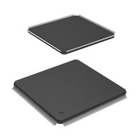
HD6417705F133BV Renesas Electronics America, HD6417705F133BV Datasheet - Page 15

HD6417705F133BV
Manufacturer Part Number
HD6417705F133BV
Description
MPU 3V 0K PB-FREE 208 FP
Manufacturer
Renesas Electronics America
Series
SuperH® SH7700r
Datasheet
1.HD6417705F133BV.pdf
(741 pages)
Specifications of HD6417705F133BV
Core Processor
SH-3
Core Size
32-Bit
Speed
133MHz
Connectivity
EBI/EMI, FIFO, IrDA, SCI, USB
Peripherals
DMA, POR, PWM, WDT
Number Of I /o
105
Program Memory Type
ROMless
Ram Size
32K x 8
Voltage - Supply (vcc/vdd)
1.4 V ~ 1.6 V
Data Converters
A/D 4x10b
Oscillator Type
Internal
Operating Temperature
-20°C ~ 75°C
Package / Case
208-LQFP
Lead Free Status / RoHS Status
Lead free / RoHS Compliant
Eeprom Size
-
Program Memory Size
-
- Current page: 15 of 741
- Download datasheet (5Mb)
Item
7.13 Others
Reset
8.3.4 DMA Channel
Control Registers (CHCR)
8.4.3 Channel Priority
Round-Robin Mode
8.4.4 DMA Transfer Types
Address Modes
Figure 8.6 Example of
DMA Transfer Timing in
Dual Mode (Source:
Ordinary Memory,
Destination: Ordinary
Memory)
Bus Mode and channel
Priority Order
8.5 Precautions
Page
237
244
245
258
262
266
270
Revisions (See Manual for Details)
In standby, sleep, and manual reset, control registers of the
bus state controller are not initialized. At manual reset, the
current bus cycle being executed is completed and then the
access wait state is entered.
counting up during manual reset signal assertion, a refresh
request occurs to initiate the refresh cycle.
Note that arbitration requests using
during manual reset signal assertion.
Bits 15, 14 description amended
00: Fixed destination address
Bits 13, 12 description amended
00: Fixed source address
CH3 immediately after a reset.
When the round-robin mode is specified, cycle-steal mode
and burst mode should not be mixed among the bus modes
for multiple channels.
Figure amended
(Active-Low)
Description largely revised
Newly added
D31 to D0
A25 to A0
DACKn
The priority of round-robin mode is CH0 > CH1 > CH2 >
CKIO
WEn
CSn
(setting prohibited in 16-byte transfer)
(setting prohibited in 16-byte transfer)
RD
Data read cycle
Transfer source
(1st cycle)
address
Rev. 2.00, 09/03, page xiii of xlvi
Since the RTCNT continues
Data write cycle
Transfer destination
(2nd cycle)
address
B R E Q
are not accepted
Related parts for HD6417705F133BV
Image
Part Number
Description
Manufacturer
Datasheet
Request
R

Part Number:
Description:
KIT STARTER FOR M16C/29
Manufacturer:
Renesas Electronics America
Datasheet:

Part Number:
Description:
KIT STARTER FOR R8C/2D
Manufacturer:
Renesas Electronics America
Datasheet:

Part Number:
Description:
R0K33062P STARTER KIT
Manufacturer:
Renesas Electronics America
Datasheet:

Part Number:
Description:
KIT STARTER FOR R8C/23 E8A
Manufacturer:
Renesas Electronics America
Datasheet:

Part Number:
Description:
KIT STARTER FOR R8C/25
Manufacturer:
Renesas Electronics America
Datasheet:

Part Number:
Description:
KIT STARTER H8S2456 SHARPE DSPLY
Manufacturer:
Renesas Electronics America
Datasheet:

Part Number:
Description:
KIT STARTER FOR R8C38C
Manufacturer:
Renesas Electronics America
Datasheet:

Part Number:
Description:
KIT STARTER FOR R8C35C
Manufacturer:
Renesas Electronics America
Datasheet:

Part Number:
Description:
KIT STARTER FOR R8CL3AC+LCD APPS
Manufacturer:
Renesas Electronics America
Datasheet:

Part Number:
Description:
KIT STARTER FOR RX610
Manufacturer:
Renesas Electronics America
Datasheet:

Part Number:
Description:
KIT STARTER FOR R32C/118
Manufacturer:
Renesas Electronics America
Datasheet:

Part Number:
Description:
KIT DEV RSK-R8C/26-29
Manufacturer:
Renesas Electronics America
Datasheet:

Part Number:
Description:
KIT STARTER FOR SH7124
Manufacturer:
Renesas Electronics America
Datasheet:

Part Number:
Description:
KIT STARTER FOR H8SX/1622
Manufacturer:
Renesas Electronics America
Datasheet:

Part Number:
Description:
KIT DEV FOR SH7203
Manufacturer:
Renesas Electronics America
Datasheet:


