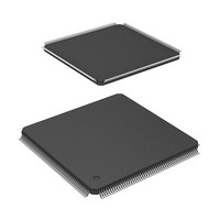
HD6417705F133BV Renesas Electronics America, HD6417705F133BV Datasheet - Page 17

HD6417705F133BV
Manufacturer Part Number
HD6417705F133BV
Description
MPU 3V 0K PB-FREE 208 FP
Manufacturer
Renesas Electronics America
Series
SuperH® SH7700r
Datasheet
1.HD6417705F133BV.pdf
(741 pages)
Specifications of HD6417705F133BV
Core Processor
SH-3
Core Size
32-Bit
Speed
133MHz
Connectivity
EBI/EMI, FIFO, IrDA, SCI, USB
Peripherals
DMA, POR, PWM, WDT
Number Of I /o
105
Program Memory Type
ROMless
Ram Size
32K x 8
Voltage - Supply (vcc/vdd)
1.4 V ~ 1.6 V
Data Converters
A/D 4x10b
Oscillator Type
Internal
Operating Temperature
-20°C ~ 75°C
Package / Case
208-LQFP
Lead Free Status / RoHS Status
Lead free / RoHS Compliant
Eeprom Size
-
Program Memory Size
-
- Current page: 17 of 741
- Download datasheet (5Mb)
Item
22.2.10 Execution Times
Break Register (BETR)
23.2 Input/Output Pins
23.3.3 Boundary Scan
Register (SDBSR)
23.5.2 Points for Attention
24.1 Register Addresses
(by functional module, in
order of the corresponding
section numbers)
Page
552
569
570
582
592
Revisions (See Manual for Details)
Note added
Note: If the channel B brake condition set to during instruction fetch cycles and any of the
Note * added
Note: * The pull-up MOS turns on if the pin function
controller (PFC) is used to select other functions (UDI).
Description amended
SDBSR is a 385-bit shift register, located on the PAD, for
controlling the input/output pins of this LSI.
Item 7 added under “23.5.2 Points for Attention”
7. The CKIO cock should operate during boundary scan.
The MD[2:0] pin should be set to the clock mode used
during normal operation, and EXTAL and CKIO should be
set within the frequency range specified in the Clock Pulse
Generator (CPG) section.
As during normal operation, the boundary scan test should
be performed after allowing sufficient settling time for the
crystal oscillator, PLL1, and PLL2.
Access size of EP1 data register and EP2 data register
amended to 8/32
instructions below perform breaks, BETR is not decremented when the first break occurs.
The decremented values are listed below.
Instruction
RTE
DMULS.L Rm,Rn
DMULU.L Rm,Rn
MAC.L @Rm+,@Rn+
MAC.W @Rm+,@Rn+
MUL.L Rm,Rn
AND.B #imm,@(R0,GBR)
OR.B #imm,@(R0,GBR)
TAS.B @Rn
TST.B #imm,@(R0,GBR)
XOR.B #imm,@(R0,GBR)
LDC Rm,SR
LDC Rm,GBR
LDC Rm,VBR
LDC Rm,SSR
LDC Rm,SPC
LDC Rm,R0_BANK
LDC Rm,R1_BANK
LDC Rm,R2_BANK
LDC Rm,R3_BANK
LDC Rm,R4_BANK
LDC Rm,R5_BANK
LDC Rm,R6_BANK
LDC Rm,R7_BANK
Value
Decremented
4
2
2
2
2
3
3
3
3
3
3
4
4
4
4
4
4
4
4
4
4
4
4
4
Rev. 2.00, 09/03, page xv of xlvi
Instruction
LDC.L @Rm+,SR
LDC.L @Rm+,GBR
LDC.L @Rm+,VBR
LDC.L @Rm+,SSR
LDC.L @Rm+,SPC
LDC.L @Rm+,R0_BANK
LDC.L @Rm+,R1_BANK
LDC.L @Rm+,R2_BANK
LDC.L @Rm+,R3_BANK
LDC.L @Rm+,R4_BANK
LDC.L @Rm+,R5_BANK
LDC.L @Rm+,R6_BANK
LDC.L @Rm+,R7_BANK
LDC.L @Rn+,MOD
LDC.L @Rn+,RS
LDC.L @Rn+,RE
LDC Rn,MOD
LDC Rn,RS
LDC Rn,RE
BSR label
BSRF Rm
JSR @Rm
Value
Decremented
6
4
4
4
4
4
4
4
4
4
4
4
4
4
4
4
4
4
4
2
2
2
Related parts for HD6417705F133BV
Image
Part Number
Description
Manufacturer
Datasheet
Request
R

Part Number:
Description:
KIT STARTER FOR M16C/29
Manufacturer:
Renesas Electronics America
Datasheet:

Part Number:
Description:
KIT STARTER FOR R8C/2D
Manufacturer:
Renesas Electronics America
Datasheet:

Part Number:
Description:
R0K33062P STARTER KIT
Manufacturer:
Renesas Electronics America
Datasheet:

Part Number:
Description:
KIT STARTER FOR R8C/23 E8A
Manufacturer:
Renesas Electronics America
Datasheet:

Part Number:
Description:
KIT STARTER FOR R8C/25
Manufacturer:
Renesas Electronics America
Datasheet:

Part Number:
Description:
KIT STARTER H8S2456 SHARPE DSPLY
Manufacturer:
Renesas Electronics America
Datasheet:

Part Number:
Description:
KIT STARTER FOR R8C38C
Manufacturer:
Renesas Electronics America
Datasheet:

Part Number:
Description:
KIT STARTER FOR R8C35C
Manufacturer:
Renesas Electronics America
Datasheet:

Part Number:
Description:
KIT STARTER FOR R8CL3AC+LCD APPS
Manufacturer:
Renesas Electronics America
Datasheet:

Part Number:
Description:
KIT STARTER FOR RX610
Manufacturer:
Renesas Electronics America
Datasheet:

Part Number:
Description:
KIT STARTER FOR R32C/118
Manufacturer:
Renesas Electronics America
Datasheet:

Part Number:
Description:
KIT DEV RSK-R8C/26-29
Manufacturer:
Renesas Electronics America
Datasheet:

Part Number:
Description:
KIT STARTER FOR SH7124
Manufacturer:
Renesas Electronics America
Datasheet:

Part Number:
Description:
KIT STARTER FOR H8SX/1622
Manufacturer:
Renesas Electronics America
Datasheet:

Part Number:
Description:
KIT DEV FOR SH7203
Manufacturer:
Renesas Electronics America
Datasheet:


