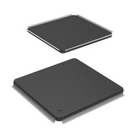
HD6417705F133BV Renesas Electronics America, HD6417705F133BV Datasheet - Page 291

HD6417705F133BV
Manufacturer Part Number
HD6417705F133BV
Description
MPU 3V 0K PB-FREE 208 FP
Manufacturer
Renesas Electronics America
Series
SuperH® SH7700r
Datasheet
1.HD6417705F133BV.pdf
(741 pages)
Specifications of HD6417705F133BV
Core Processor
SH-3
Core Size
32-Bit
Speed
133MHz
Connectivity
EBI/EMI, FIFO, IrDA, SCI, USB
Peripherals
DMA, POR, PWM, WDT
Number Of I /o
105
Program Memory Type
ROMless
Ram Size
32K x 8
Voltage - Supply (vcc/vdd)
1.4 V ~ 1.6 V
Data Converters
A/D 4x10b
Oscillator Type
Internal
Operating Temperature
-20°C ~ 75°C
Package / Case
208-LQFP
Lead Free Status / RoHS Status
Lead free / RoHS Compliant
Eeprom Size
-
Program Memory Size
-
- Current page: 291 of 741
- Download datasheet (5Mb)
8.3.3
DMATCR are 32-bit readable/writable registers that specify the DMA transfer count. The number
of transfers is 1 when the setting is H'00000001, 16,777,215 when H'00FFFFFF is set, and
16,777,216 (the maximum) when H'00000000 is set. During a DMA transfer, these registers
indicate the remaining transfer count.
The upper 8 bits of DMATCR are always read as 0. The write value should always be 0. To
transfer data in 16 bytes, one 16-byte transfer (128 bits) counts one. The initial value is undefined.
The DMATCR retains the current value in software standby or module standby mode.
8.3.4
CHCR are 32-bit readable/writable registers that control the DMA transfer mode.
Bit
31 to 24
23
22
21 to 18
Bit
Name
DO
TL
DMA Transfer Count Registers (DMATCR)
DMA Channel Control Registers (CHCR)
Initial
Value
0
0
0
0
R/W
R
R/W
R/W
R
Descriptions
Reserved
These bits are always read as 0. The write value should always
be 0.
DMA Overrun
Selects whether DREQ is detected by overrun 0 or by overrun
1. This bit is valid only in CHCR_0 and CHCR_1. This bit is
always read as 0 in CHCR_2 and CHCR_3. The write value
should always be 0.
0: Detects DREQ by overrun 0
1: Detects DREQ by overrun 1
Transfer End Level
Selects whether the TEND signal output is high active or low
active. This bit is valid only in CHCR_0. There are no TEND
pins in CHCR_1 to CHCR_3. Therefore this setting is invalid.
This bit is always read as 0. The write value should always be
0.
0: Low-active output of TEND
1: High-active output of TEND
Reserved
These bits are always read as 0. The write value should always
be 0.
Rev. 2.00, 09/03, page 243 of 690
Related parts for HD6417705F133BV
Image
Part Number
Description
Manufacturer
Datasheet
Request
R

Part Number:
Description:
KIT STARTER FOR M16C/29
Manufacturer:
Renesas Electronics America
Datasheet:

Part Number:
Description:
KIT STARTER FOR R8C/2D
Manufacturer:
Renesas Electronics America
Datasheet:

Part Number:
Description:
R0K33062P STARTER KIT
Manufacturer:
Renesas Electronics America
Datasheet:

Part Number:
Description:
KIT STARTER FOR R8C/23 E8A
Manufacturer:
Renesas Electronics America
Datasheet:

Part Number:
Description:
KIT STARTER FOR R8C/25
Manufacturer:
Renesas Electronics America
Datasheet:

Part Number:
Description:
KIT STARTER H8S2456 SHARPE DSPLY
Manufacturer:
Renesas Electronics America
Datasheet:

Part Number:
Description:
KIT STARTER FOR R8C38C
Manufacturer:
Renesas Electronics America
Datasheet:

Part Number:
Description:
KIT STARTER FOR R8C35C
Manufacturer:
Renesas Electronics America
Datasheet:

Part Number:
Description:
KIT STARTER FOR R8CL3AC+LCD APPS
Manufacturer:
Renesas Electronics America
Datasheet:

Part Number:
Description:
KIT STARTER FOR RX610
Manufacturer:
Renesas Electronics America
Datasheet:

Part Number:
Description:
KIT STARTER FOR R32C/118
Manufacturer:
Renesas Electronics America
Datasheet:

Part Number:
Description:
KIT DEV RSK-R8C/26-29
Manufacturer:
Renesas Electronics America
Datasheet:

Part Number:
Description:
KIT STARTER FOR SH7124
Manufacturer:
Renesas Electronics America
Datasheet:

Part Number:
Description:
KIT STARTER FOR H8SX/1622
Manufacturer:
Renesas Electronics America
Datasheet:

Part Number:
Description:
KIT DEV FOR SH7203
Manufacturer:
Renesas Electronics America
Datasheet:


