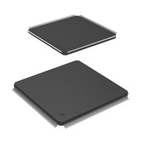
HD6417705F133BV Renesas Electronics America, HD6417705F133BV Datasheet - Page 261

HD6417705F133BV
Manufacturer Part Number
HD6417705F133BV
Description
MPU 3V 0K PB-FREE 208 FP
Manufacturer
Renesas Electronics America
Series
SuperH® SH7700r
Datasheet
1.HD6417705F133BV.pdf
(741 pages)
Specifications of HD6417705F133BV
Core Processor
SH-3
Core Size
32-Bit
Speed
133MHz
Connectivity
EBI/EMI, FIFO, IrDA, SCI, USB
Peripherals
DMA, POR, PWM, WDT
Number Of I /o
105
Program Memory Type
ROMless
Ram Size
32K x 8
Voltage - Supply (vcc/vdd)
1.4 V ~ 1.6 V
Data Converters
A/D 4x10b
Oscillator Type
Internal
Operating Temperature
-20°C ~ 75°C
Package / Case
208-LQFP
Lead Free Status / RoHS Status
Lead free / RoHS Compliant
Eeprom Size
-
Program Memory Size
-
- Current page: 261 of 741
- Download datasheet (5Mb)
Figure 7.16 shows a timing chart in burst read. In burst read, an ACTV command is output in the
Tr cycle, the READ command is issued in the Tc1, Tc2, and Tc3 cycles, the READA command is
issued in the Tc4 cycle, and the read data is received at the rising edge of the external clock
(CKIO) in the Td1 to Td4 cycles. The Tap cycle is used to wait for the completion of an auto-
precharge induced by the READ command in the SDRAM. In the Tap cycle, a new command
will not be issued to the same bank. However, access to another CS space or another bank in the
same SDRAM space is enabled. The number of Tap cycles is specified by the TRP[1:0] bits of
the CS3WCR register.
A12/A11 *
D31 to D0
A25 to A0
DACKn *
DQMxx *
RD/WR
RASU/L
CASU/L
CKIO
CSn
BS
1
3
Figure 7.16 Synchronous DRAM Burst Read Wait Specification Timing
2
Notes: 1. Address pin to be connected to the A10 pin of SDRAM.
2. xx is UU, UL, LU, or LL.
3. The waveform for DACKn is when active low is specified.
Tr
Trw
Tc1
(Auto Precharge)
Tc2
Tw
Td1
Tc3
Td2
Tc4
Td3
Rev. 2.00, 09/03, page 213 of 690
Td4
Tde
Tap
Related parts for HD6417705F133BV
Image
Part Number
Description
Manufacturer
Datasheet
Request
R

Part Number:
Description:
KIT STARTER FOR M16C/29
Manufacturer:
Renesas Electronics America
Datasheet:

Part Number:
Description:
KIT STARTER FOR R8C/2D
Manufacturer:
Renesas Electronics America
Datasheet:

Part Number:
Description:
R0K33062P STARTER KIT
Manufacturer:
Renesas Electronics America
Datasheet:

Part Number:
Description:
KIT STARTER FOR R8C/23 E8A
Manufacturer:
Renesas Electronics America
Datasheet:

Part Number:
Description:
KIT STARTER FOR R8C/25
Manufacturer:
Renesas Electronics America
Datasheet:

Part Number:
Description:
KIT STARTER H8S2456 SHARPE DSPLY
Manufacturer:
Renesas Electronics America
Datasheet:

Part Number:
Description:
KIT STARTER FOR R8C38C
Manufacturer:
Renesas Electronics America
Datasheet:

Part Number:
Description:
KIT STARTER FOR R8C35C
Manufacturer:
Renesas Electronics America
Datasheet:

Part Number:
Description:
KIT STARTER FOR R8CL3AC+LCD APPS
Manufacturer:
Renesas Electronics America
Datasheet:

Part Number:
Description:
KIT STARTER FOR RX610
Manufacturer:
Renesas Electronics America
Datasheet:

Part Number:
Description:
KIT STARTER FOR R32C/118
Manufacturer:
Renesas Electronics America
Datasheet:

Part Number:
Description:
KIT DEV RSK-R8C/26-29
Manufacturer:
Renesas Electronics America
Datasheet:

Part Number:
Description:
KIT STARTER FOR SH7124
Manufacturer:
Renesas Electronics America
Datasheet:

Part Number:
Description:
KIT STARTER FOR H8SX/1622
Manufacturer:
Renesas Electronics America
Datasheet:

Part Number:
Description:
KIT DEV FOR SH7203
Manufacturer:
Renesas Electronics America
Datasheet:


