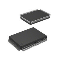
DF2367VF33 Renesas Electronics America, DF2367VF33 Datasheet - Page 909

DF2367VF33
Manufacturer Part Number
DF2367VF33
Description
MCU 3V 384K 128-QFP
Manufacturer
Renesas Electronics America
Series
H8® H8S/2300r
Datasheet
1.DF2368VTE34V.pdf
(1044 pages)
Specifications of DF2367VF33
Core Processor
H8S/2000
Core Size
16-Bit
Speed
33MHz
Connectivity
I²C, IrDA, SCI, SmartCard
Peripherals
DMA, POR, PWM, WDT
Number Of I /o
84
Program Memory Size
384KB (384K x 8)
Program Memory Type
FLASH
Ram Size
24K x 8
Voltage - Supply (vcc/vdd)
3 V ~ 3.6 V
Data Converters
A/D 10x10b, D/A 2x8b
Oscillator Type
Internal
Operating Temperature
-20°C ~ 75°C
Package / Case
128-QFP
Lead Free Status / RoHS Status
Contains lead / RoHS non-compliant
Eeprom Size
-
Other names
HD64F2367VF33
HD64F2367VF33
HD64F2367VF33
Available stocks
Company
Part Number
Manufacturer
Quantity
Price
Company:
Part Number:
DF2367VF33V
Manufacturer:
Renesas Electronics America
Quantity:
135
Company:
Part Number:
DF2367VF33V
Manufacturer:
Renesas Electronics America
Quantity:
10 000
Company:
Part Number:
DF2367VF33WV
Manufacturer:
Renesas Electronics America
Quantity:
10 000
- Current page: 909 of 1044
- Download datasheet (6Mb)
Register Name
Timer general register C_0
Timer general register D_0
Timer control register_1
Timer mode register_1
Timer I/O control register_1
Timer interrupt enable register_1
Timer status register_1
Timer counter_1
Timer general register A_1
Timer general register B_1
Timer control register_2
Timer mode register_2
Timer I/O control register_2
Timer interrupt enable register_2
Timer status rgister_2
Timer counter_2
Timer general register A_2
Timer general register B_2
Notes: 1.
2. For writing, refer to section 13.6.1, Notes on Register Access.
3. Supported only by the H8S/2368 0.18 μm F-ZTAT Group.
4. Cannot be accessed by other than H8S/2368 0.18 μm F-ZTAT Group.
If the pulse output group 2 and pulse output group 3 output triggers are the same
according to the PCR setting, the NDRH address will be H'FF4C, and if different, the
address of NDRH for group 2 will be H'FF4E, and that for group 3 will be H'FF4C.
Similarly, if the pulse output group 0 and pulse output group 1 output triggers are the
same according to the PCR setting, the NDRL address will be H'FF4D, and if different,
the address of NDRL for group 0 will be H'FF4F, and that for group 1 will be H'FF4D.
Abbrevia-
tion
TGRC_0
TGRD_0
TCR_1
TMDR_1
TIOR_1
TIER_1
TSR_1
TCNT_1
TGRA_1
TGRB_1
TCR_2
TMDR_2
TIOR_2
TIER_2
TSR_2
TCNT_2
TGRA_2
TGRB_2
Bit No. Address Module
16
16
8
8
8
8
8
16
16
16
8
8
8
8
8
16
16
16
Rev.6.00 Mar. 18, 2009 Page 849 of 980
H'FFDC
H'FFDE
H'FFE0
H'FFE1
H'FFE2
H'FFE4
H'FFE5
H'FFE6
H'FFE8
H'FFEA
H'FFF0
H'FFF1
H'FFF2
H'FFF4
H'FFF5
H'FFF6
H'FFF8
H'FFFA
TPU_0
TPU_0
TPU_1
TPU_1
TPU_1
TPU_1
TPU_1
TPU_1
TPU_1
TPU_1
TPU_2
TPU_2
TPU_2
TPU_2
TPU_2
TPU_2
TPU_2
TPU_2
Section 24 List of Registers
Data
Width
16
16
16
16
16
16
16
16
16
16
16
16
16
16
16
16
16
16
REJ09B0050-0600
Access
States
2
2
2
2
2
2
2
2
2
2
2
2
2
2
2
2
2
2
Related parts for DF2367VF33
Image
Part Number
Description
Manufacturer
Datasheet
Request
R

Part Number:
Description:
CONN PLUG 12POS DUAL 0.5MM SMD
Manufacturer:
Hirose Electric Co Ltd
Datasheet:

Part Number:
Description:
CONN PLUG 18POS DUAL 0.5MM SMD
Manufacturer:
Hirose Electric Co Ltd
Datasheet:

Part Number:
Description:
CONN PLUG 14POS DUAL 0.5MM SMD
Manufacturer:
Hirose Electric Co Ltd
Datasheet:

Part Number:
Description:
CONN RECEPT 20POS DUAL 0.5MM SMD
Manufacturer:
Hirose Electric Co Ltd
Datasheet:

Part Number:
Description:
CONN PLUG 16POS DUAL 0.5MM SMD
Manufacturer:
Hirose Electric Co Ltd
Datasheet:

Part Number:
Description:
CONN RECEPT 16POS DUAL 0.5MM SMD
Manufacturer:
Hirose Electric Co Ltd
Datasheet:

Part Number:
Description:
CONN PLUG 20POS DUAL 0.5MM SMD
Manufacturer:
Hirose Electric Co Ltd
Datasheet:

Part Number:
Description:
CONN PLUG 30POS DUAL 0.5MM SMD
Manufacturer:
Hirose Electric Co Ltd
Datasheet:

Part Number:
Description:
CONN RECEPT 30POS DUAL 0.5MM SMD
Manufacturer:
Hirose Electric Co Ltd
Datasheet:

Part Number:
Description:
CONN PLUG 40POS DUAL 0.5MM SMD
Manufacturer:
Hirose Electric Co Ltd
Datasheet:

Part Number:
Description:
KIT STARTER FOR M16C/29
Manufacturer:
Renesas Electronics America
Datasheet:

Part Number:
Description:
KIT STARTER FOR R8C/2D
Manufacturer:
Renesas Electronics America
Datasheet:

Part Number:
Description:
R0K33062P STARTER KIT
Manufacturer:
Renesas Electronics America
Datasheet:

Part Number:
Description:
KIT STARTER FOR R8C/23 E8A
Manufacturer:
Renesas Electronics America
Datasheet:

Part Number:
Description:
KIT STARTER FOR R8C/25
Manufacturer:
Renesas Electronics America
Datasheet:


