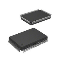
DF2367VF33 Renesas Electronics America, DF2367VF33 Datasheet - Page 989

DF2367VF33
Manufacturer Part Number
DF2367VF33
Description
MCU 3V 384K 128-QFP
Manufacturer
Renesas Electronics America
Series
H8® H8S/2300r
Datasheet
1.DF2368VTE34V.pdf
(1044 pages)
Specifications of DF2367VF33
Core Processor
H8S/2000
Core Size
16-Bit
Speed
33MHz
Connectivity
I²C, IrDA, SCI, SmartCard
Peripherals
DMA, POR, PWM, WDT
Number Of I /o
84
Program Memory Size
384KB (384K x 8)
Program Memory Type
FLASH
Ram Size
24K x 8
Voltage - Supply (vcc/vdd)
3 V ~ 3.6 V
Data Converters
A/D 10x10b, D/A 2x8b
Oscillator Type
Internal
Operating Temperature
-20°C ~ 75°C
Package / Case
128-QFP
Lead Free Status / RoHS Status
Contains lead / RoHS non-compliant
Eeprom Size
-
Other names
HD64F2367VF33
HD64F2367VF33
HD64F2367VF33
Available stocks
Company
Part Number
Manufacturer
Quantity
Price
Company:
Part Number:
DF2367VF33V
Manufacturer:
Renesas Electronics America
Quantity:
135
Company:
Part Number:
DF2367VF33V
Manufacturer:
Renesas Electronics America
Quantity:
10 000
Company:
Part Number:
DF2367VF33WV
Manufacturer:
Renesas Electronics America
Quantity:
10 000
- Current page: 989 of 1044
- Download datasheet (6Mb)
Notes: 1. When the A/D and D/A converters are not used, the AV
Table 25.29 Permissible Output Currents
Conditions: V
Item
Permissible output low
current (per pin)
Permissible output low
current (total)
Permissible output high
current (per pin)
Permissible output high
current (total)
Caution:
Note:
Item
V
CC
rise slope *
2. Current consumption values are for V
3. The values are for V
4. I
5. Applies when the RES pin is at low level at power-on.
*
I
I
be open. Connect the AV
output pins unloaded and all input pull-up MOSs in the off state.
To protect the LSI’s reliability, do not exceed the output current values in table 25.29.
When the A/D and D/A converters are not used, do not leave the AV
pins should not be open. Connect the AV
CC
CC
CC
max = 15 (mA) + 0.37 (mA/(MHz × V)) × V
max = 15 (mA) + 0.20 (mA/(MHz × V)) × V
V
T
depends on V
5
a
CC
SS
= −40°C to +85°C (wide-range specifications)
= AV
= 3.0 V to 3.6 V, AV
SS
= 0 V*, T
SCL0 to SCL1, SDA0 to SDA1
Output pins other than the above
Total of all output pins
All output pins
Total of all output pins
CC
and f as follows:
RAM
Symbol
SV
a
≤ V
CC
= −20°C to +75°C (regular specifications),
CC
CC
CC
and V
< 3.0 V, V
= 3.0 V to 3.6 V, V
Min.
⎯
ref
pins to V
IH
min = V
IH
min = V
CC
and V
CC
CC
CC
Typ.
⎯
, and the AV
Rev.6.00 Mar. 18, 2009 Page 929 of 980
CC
× f (normal operation)
× f (sleep mode)
CC
− 0.2 V and V
ref
ref
Symbol
I
ΣI
−I
Σ−I
× 0.9, and V
OL
Section 25 Electrical Characteristics
= 3.0 V to AV
pins to V
OL
OH
OH
CC
, V
Max.
⎯
SS
ref
⎯
⎯
⎯
⎯
⎯
CC
Min.
pin to V
, and AV
, and the AV
IL
IL
max = 0.3 V.
max = 0.2 V with all
CC
Unit
ms/V
Typ. Max. Unit
⎯
⎯
⎯
⎯
⎯
,
SS
CC
REJ09B0050-0600
.
SS
, V
pins should not
ref
Test
Conditions
, and AV
SS
8.0
2.0
80
2.0
40
pin to V
mA
mA
mA
mA
SS
SS
.
Related parts for DF2367VF33
Image
Part Number
Description
Manufacturer
Datasheet
Request
R

Part Number:
Description:
CONN PLUG 12POS DUAL 0.5MM SMD
Manufacturer:
Hirose Electric Co Ltd
Datasheet:

Part Number:
Description:
CONN PLUG 18POS DUAL 0.5MM SMD
Manufacturer:
Hirose Electric Co Ltd
Datasheet:

Part Number:
Description:
CONN PLUG 14POS DUAL 0.5MM SMD
Manufacturer:
Hirose Electric Co Ltd
Datasheet:

Part Number:
Description:
CONN RECEPT 20POS DUAL 0.5MM SMD
Manufacturer:
Hirose Electric Co Ltd
Datasheet:

Part Number:
Description:
CONN PLUG 16POS DUAL 0.5MM SMD
Manufacturer:
Hirose Electric Co Ltd
Datasheet:

Part Number:
Description:
CONN RECEPT 16POS DUAL 0.5MM SMD
Manufacturer:
Hirose Electric Co Ltd
Datasheet:

Part Number:
Description:
CONN PLUG 20POS DUAL 0.5MM SMD
Manufacturer:
Hirose Electric Co Ltd
Datasheet:

Part Number:
Description:
CONN PLUG 30POS DUAL 0.5MM SMD
Manufacturer:
Hirose Electric Co Ltd
Datasheet:

Part Number:
Description:
CONN RECEPT 30POS DUAL 0.5MM SMD
Manufacturer:
Hirose Electric Co Ltd
Datasheet:

Part Number:
Description:
CONN PLUG 40POS DUAL 0.5MM SMD
Manufacturer:
Hirose Electric Co Ltd
Datasheet:

Part Number:
Description:
KIT STARTER FOR M16C/29
Manufacturer:
Renesas Electronics America
Datasheet:

Part Number:
Description:
KIT STARTER FOR R8C/2D
Manufacturer:
Renesas Electronics America
Datasheet:

Part Number:
Description:
R0K33062P STARTER KIT
Manufacturer:
Renesas Electronics America
Datasheet:

Part Number:
Description:
KIT STARTER FOR R8C/23 E8A
Manufacturer:
Renesas Electronics America
Datasheet:

Part Number:
Description:
KIT STARTER FOR R8C/25
Manufacturer:
Renesas Electronics America
Datasheet:


