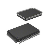
DF2367VF33 Renesas Electronics America, DF2367VF33 Datasheet - Page 981

DF2367VF33
Manufacturer Part Number
DF2367VF33
Description
MCU 3V 384K 128-QFP
Manufacturer
Renesas Electronics America
Series
H8® H8S/2300r
Datasheet
1.DF2368VTE34V.pdf
(1044 pages)
Specifications of DF2367VF33
Core Processor
H8S/2000
Core Size
16-Bit
Speed
33MHz
Connectivity
I²C, IrDA, SCI, SmartCard
Peripherals
DMA, POR, PWM, WDT
Number Of I /o
84
Program Memory Size
384KB (384K x 8)
Program Memory Type
FLASH
Ram Size
24K x 8
Voltage - Supply (vcc/vdd)
3 V ~ 3.6 V
Data Converters
A/D 10x10b, D/A 2x8b
Oscillator Type
Internal
Operating Temperature
-20°C ~ 75°C
Package / Case
128-QFP
Lead Free Status / RoHS Status
Contains lead / RoHS non-compliant
Eeprom Size
-
Other names
HD64F2367VF33
HD64F2367VF33
HD64F2367VF33
Available stocks
Company
Part Number
Manufacturer
Quantity
Price
Company:
Part Number:
DF2367VF33V
Manufacturer:
Renesas Electronics America
Quantity:
135
Company:
Part Number:
DF2367VF33V
Manufacturer:
Renesas Electronics America
Quantity:
10 000
Company:
Part Number:
DF2367VF33WV
Manufacturer:
Renesas Electronics America
Quantity:
10 000
- Current page: 981 of 1044
- Download datasheet (6Mb)
(5) Timing of On-Chip Peripheral Modules
Table 25.22 Timing of On-Chip Peripheral Modules
Conditions: V
Item
I/O ports
PPG
TPU
8-bit timer
WDT
SCI
A/D
converter
Output data delay time
Input data setup time
Input data hold time
Pulse output delay time
Timer output delay time
Timer input setup time
Timer clock input setup time t
Timer clock
pulse width
Timer output delay time
Timer reset input setup time t
Timer clock input setup time t
Timer clock
pulse width
Overflow output delay time
Input clock
cycle
Input clock pulse width
Input clock rise time
Input clock fall time
Transmit data delay time
Receive data setup time
(synchronous)
Receive data hold time
(synchronous)
Trigger input setup time
φ = 8 MHz to 33 MHz, T
T
a
CC
= –40°C to +85°C (wide-range specifications)
= 3.0 V to 3.6 V, AV
Asynchronous
Single-edge
specification
Both-edge
specification
Single-edge
specification
Both-edge
specification
Synchronous
CC
a
= –20°C to +75°C (regular specifications),
= 3.0 V to 3.6 V, V
Symbol Min
t
t
t
t
t
t
t
t
t
t
t
t
t
t
t
t
t
t
t
t
PWD
PRS
PRH
POD
TOCD
TICS
TCKS
TCKWH
TCKWL
TMOD
TMRS
TMCS
TMCWH
TMCWL
WOVD
Scyc
SCKW
SCKr
SCKf
TXD
RXS
RXH
TRGS
—
25
25
—
—
25
25
1.5
2.5
—
25
25
1.5
2.5
—
4
6
0.4
—
—
—
40
40
30
Rev.6.00 Mar. 18, 2009 Page 921 of 980
ref
Section 25 Electrical Characteristics
= 3.0 V to AV
Max
40
—
—
40
40
—
—
—
—
40
—
—
—
—
40
—
—
0.6
1.5
1.5
40
—
—
—
Unit
ns
ns
ns
ns
ns
ns
ns
t
t
ns
ns
ns
t
t
ns
t
t
t
ns
ns
ns
ns
cyc
cyc
cyc
cyc
cyc
Scyc
cyc
CC
, V
REJ09B0050-0600
Test Conditions
Figure 25.28
Figure 25.29
Figure 25.30
Figure 25.31
Figure 25.32
Figure 25.34
Figure 25.33
Figure 25.35
Figure 25.36
Figure 25.37
Figure 25.38
SS
= AV
SS
= 0 V,
Related parts for DF2367VF33
Image
Part Number
Description
Manufacturer
Datasheet
Request
R

Part Number:
Description:
CONN PLUG 12POS DUAL 0.5MM SMD
Manufacturer:
Hirose Electric Co Ltd
Datasheet:

Part Number:
Description:
CONN PLUG 18POS DUAL 0.5MM SMD
Manufacturer:
Hirose Electric Co Ltd
Datasheet:

Part Number:
Description:
CONN PLUG 14POS DUAL 0.5MM SMD
Manufacturer:
Hirose Electric Co Ltd
Datasheet:

Part Number:
Description:
CONN RECEPT 20POS DUAL 0.5MM SMD
Manufacturer:
Hirose Electric Co Ltd
Datasheet:

Part Number:
Description:
CONN PLUG 16POS DUAL 0.5MM SMD
Manufacturer:
Hirose Electric Co Ltd
Datasheet:

Part Number:
Description:
CONN RECEPT 16POS DUAL 0.5MM SMD
Manufacturer:
Hirose Electric Co Ltd
Datasheet:

Part Number:
Description:
CONN PLUG 20POS DUAL 0.5MM SMD
Manufacturer:
Hirose Electric Co Ltd
Datasheet:

Part Number:
Description:
CONN PLUG 30POS DUAL 0.5MM SMD
Manufacturer:
Hirose Electric Co Ltd
Datasheet:

Part Number:
Description:
CONN RECEPT 30POS DUAL 0.5MM SMD
Manufacturer:
Hirose Electric Co Ltd
Datasheet:

Part Number:
Description:
CONN PLUG 40POS DUAL 0.5MM SMD
Manufacturer:
Hirose Electric Co Ltd
Datasheet:

Part Number:
Description:
KIT STARTER FOR M16C/29
Manufacturer:
Renesas Electronics America
Datasheet:

Part Number:
Description:
KIT STARTER FOR R8C/2D
Manufacturer:
Renesas Electronics America
Datasheet:

Part Number:
Description:
R0K33062P STARTER KIT
Manufacturer:
Renesas Electronics America
Datasheet:

Part Number:
Description:
KIT STARTER FOR R8C/23 E8A
Manufacturer:
Renesas Electronics America
Datasheet:

Part Number:
Description:
KIT STARTER FOR R8C/25
Manufacturer:
Renesas Electronics America
Datasheet:


