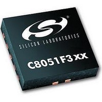
C8051F302 Silicon Laboratories Inc, C8051F302 Datasheet - Page 125

C8051F302
Manufacturer Part Number
C8051F302
Description
IC 8051 MCU 8K FLASH 11MLP
Manufacturer
Silicon Laboratories Inc
Series
C8051F30xr
Specifications of C8051F302
Core Processor
8051
Core Size
8-Bit
Speed
25MHz
Connectivity
SMBus (2-Wire/I²C), UART/USART
Peripherals
POR, PWM, Temp Sensor, WDT
Number Of I /o
8
Program Memory Size
8KB (8K x 8)
Program Memory Type
FLASH
Ram Size
256 x 8
Voltage - Supply (vcc/vdd)
2.7 V ~ 3.6 V
Data Converters
A/D 8x8b
Oscillator Type
External
Operating Temperature
-40°C ~ 85°C
Package / Case
11-VQFN
Data Bus Width
8 bit
Data Ram Size
256 B
Interface Type
I2C, SMBus, UART
Maximum Clock Frequency
25 MHz
Number Of Programmable I/os
8
Number Of Timers
16 bit
Operating Supply Voltage
2.7 V to 3.6 V
Maximum Operating Temperature
+ 85 C
Mounting Style
SMD/SMT
Minimum Operating Temperature
- 40 C
On-chip Adc
8 bit
Lead Free Status / RoHS Status
Contains lead / RoHS non-compliant
Eeprom Size
-
Lead Free Status / Rohs Status
No
Available stocks
Company
Part Number
Manufacturer
Quantity
Price
Company:
Part Number:
C8051F302-GMR
Manufacturer:
SiliconL
Quantity:
3 000
Company:
Part Number:
C8051F302-GMR
Manufacturer:
SILICON
Quantity:
5 000
Part Number:
C8051F302-GMR
Manufacturer:
SILICONLABS/èٹ¯ç§‘
Quantity:
20 000
14.2. Operational Modes
UART0 provides standard asynchronous, full duplex communication. The UART mode (8-bit or 9-bit) is selected by
the S0MODE bit (SCON0.7). Typical UART connection options are shown below.
14.2.1. 8-Bit UART
8-Bit UART mode uses a total of 10 bits per data byte: one start bit, eight data bits (LSB first), and one stop bit. Data
are transmitted LSB first from the TX pin and received at the RX pin. On receive, the eight data bits are stored in
SBUF0 and the stop bit goes into RB80 (SCON0.2).
Data transmission begins when software writes a data byte to the SBUF0 register. The TI0 Transmit Interrupt Flag
(SCON0.1) is set at the end of the transmission (the beginning of the stop-bit time). Data reception can begin any
time after the REN0 Receive Enable bit (SCON0.4) is set to logic 1. After the stop bit is received, the data byte will
be loaded into the SBUF0 receive register if the following conditions are met: RI0 must be logic 0, and if MCE0 is
logic 1, the stop bit must be logic 1. In the event of a receive data overrun, the first received 8 bits are latched into the
SBUF0 receive register and the following overrun data bits are lost.
If these conditions are met, the eight bits of data is stored in SBUF0, the stop bit is stored in RB80 and the RI0 flag is
set. If these conditions are not met, SBUF0 and RB80 will not be loaded and the RI0 flag will not be set. An interrupt
will occur if enabled when either TI0 or RI0 is set.
SPACE
MARK
BIT TIMES
BIT SAMPLING
START
BIT
D0
Figure 14.4. 8-Bit UART Timing Diagram
Figure 14.3. UART Interconnect Diagram
D1
RS-232
MCU
D2
TX
RX
D3
Rev. 2.3
RS-232
LEVEL
XLTR
OR
D4
RX
RX
TX
TX
C8051Fxxx
C8051F300/1/2/3/4/5
D5
C8051Fxxx
D6
D7
STOP
BIT
125


