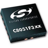
C8051F302 Silicon Laboratories Inc, C8051F302 Datasheet - Page 91

C8051F302
Manufacturer Part Number
C8051F302
Description
IC 8051 MCU 8K FLASH 11MLP
Manufacturer
Silicon Laboratories Inc
Series
C8051F30xr
Specifications of C8051F302
Core Processor
8051
Core Size
8-Bit
Speed
25MHz
Connectivity
SMBus (2-Wire/I²C), UART/USART
Peripherals
POR, PWM, Temp Sensor, WDT
Number Of I /o
8
Program Memory Size
8KB (8K x 8)
Program Memory Type
FLASH
Ram Size
256 x 8
Voltage - Supply (vcc/vdd)
2.7 V ~ 3.6 V
Data Converters
A/D 8x8b
Oscillator Type
External
Operating Temperature
-40°C ~ 85°C
Package / Case
11-VQFN
Data Bus Width
8 bit
Data Ram Size
256 B
Interface Type
I2C, SMBus, UART
Maximum Clock Frequency
25 MHz
Number Of Programmable I/os
8
Number Of Timers
16 bit
Operating Supply Voltage
2.7 V to 3.6 V
Maximum Operating Temperature
+ 85 C
Mounting Style
SMD/SMT
Minimum Operating Temperature
- 40 C
On-chip Adc
8 bit
Lead Free Status / RoHS Status
Contains lead / RoHS non-compliant
Eeprom Size
-
Lead Free Status / Rohs Status
No
Available stocks
Company
Part Number
Manufacturer
Quantity
Price
Company:
Part Number:
C8051F302-GMR
Manufacturer:
SiliconL
Quantity:
3 000
Company:
Part Number:
C8051F302-GMR
Manufacturer:
SILICON
Quantity:
5 000
Part Number:
C8051F302-GMR
Manufacturer:
SILICONLABS/èٹ¯ç§‘
Quantity:
20 000
11.2.
The external oscillator circuit may drive an external crystal, ceramic resonator, capacitor, or RC network. A CMOS
clock may also provide a clock input. For a crystal or ceramic resonator configuration, the crystal/resonator must be
wired across the XTAL1 and XTAL2 pins as shown in Option 1 of Figure 11.1. A 10 MΩ resistor also must be wired
across the XTAL2 and XTAL1 pins for the crystal/resonator configuration. In RC, capacitor, or CMOS clock config-
uration, the clock source should be wired to the XTAL2 pin as shown in Option 2, 3, or 4 of Figure 11.1. The type of
external oscillator must be selected in the OSCXCN register, and the frequency control bits (XFCN) must be selected
appropriately (see Figure 11.4).
Important Note on External Oscillator Usage: Port pins must be configured when using the external oscillator cir-
cuit. When the external oscillator drive circuit is enabled in crystal/resonator mode, Port pins P0.2 and P0.3 are occu-
pied as XTAL1 and XTAL2 respectively. When the external oscillator drive circuit is enabled in capacitor, RC, or
CMOS clock mode, Port pin P0.3 is occupied as XTAL2. The Port I/O Crossbar should be configured to skip the
occupied Port pins; see
tionally, when using the external oscillator circuit in crystal/resonator, capacitor, or RC mode, the associated Port pins
should be configured as analog inputs. In CMOS clock mode, the associated pin should be configured as a digital
input. See
11.3.
The CLKSL bit in register OSCICN selects which oscillator is used as the system clock. CLKSL must be set to ‘1’ for
the system clock to run from the external oscillator; however the external oscillator may still clock peripherals (tim-
ers, PCA) when the internal oscillator is selected as the system clock. The system clock may be switched on-the-fly
between the internal and external oscillator, so long as the selected oscillator is enabled and has settled. The internal
oscillator requires little start-up time and may be enabled and selected as the system clock in the same write to
OSCICN. External crystals and ceramic resonators typically require a start-up time before they are settled and ready
for use as the system clock. The Crystal Valid Flag (XTLVLD in register OSCXCN) is set to ‘1’ by hardware when
the external oscillator is settled. To avoid reading a false XTLVLD, in crystal mode software should delay at least
1 ms between enabling the external oscillator and checking XTLVLD. RC and C modes typically require no startup
time.
-40°C to +85°C unless otherwise specified
Internal Oscillator Supply Current
Uncalibrated Internal Oscillator
Calibrated Internal Oscillator
External Oscillator Drive Circuit
System Clock Selection
PARAMETER
Section “12.2. Port I/O Initialization” on page 98
(from VDD)
Frequency
Frequency
Table 11.1. Internal Oscillator Electrical Characteristics
Section “12.1. Priority Crossbar Decoder” on page 96
C8051F302/3/4/5 devices
C8051F300/1 devices
CONDITIONS
OSCICN.2 = 1
Rev. 2.3
for details on Port input mode selection.
C8051F300/1/2/3/4/5
MIN
24
16
for Crossbar configuration. Addi-
TYP
24.5
450
20
MAX
25
24
UNITS
MHz
MHz
µA
91


