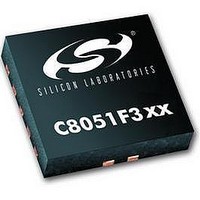
C8051F302 Silicon Laboratories Inc, C8051F302 Datasheet - Page 37

C8051F302
Manufacturer Part Number
C8051F302
Description
IC 8051 MCU 8K FLASH 11MLP
Manufacturer
Silicon Laboratories Inc
Series
C8051F30xr
Specifications of C8051F302
Core Processor
8051
Core Size
8-Bit
Speed
25MHz
Connectivity
SMBus (2-Wire/I²C), UART/USART
Peripherals
POR, PWM, Temp Sensor, WDT
Number Of I /o
8
Program Memory Size
8KB (8K x 8)
Program Memory Type
FLASH
Ram Size
256 x 8
Voltage - Supply (vcc/vdd)
2.7 V ~ 3.6 V
Data Converters
A/D 8x8b
Oscillator Type
External
Operating Temperature
-40°C ~ 85°C
Package / Case
11-VQFN
Data Bus Width
8 bit
Data Ram Size
256 B
Interface Type
I2C, SMBus, UART
Maximum Clock Frequency
25 MHz
Number Of Programmable I/os
8
Number Of Timers
16 bit
Operating Supply Voltage
2.7 V to 3.6 V
Maximum Operating Temperature
+ 85 C
Mounting Style
SMD/SMT
Minimum Operating Temperature
- 40 C
On-chip Adc
8 bit
Lead Free Status / RoHS Status
Contains lead / RoHS non-compliant
Eeprom Size
-
Lead Free Status / Rohs Status
No
Available stocks
Company
Part Number
Manufacturer
Quantity
Price
Company:
Part Number:
C8051F302-GMR
Manufacturer:
SiliconL
Quantity:
3 000
Company:
Part Number:
C8051F302-GMR
Manufacturer:
SILICON
Quantity:
5 000
Part Number:
C8051F302-GMR
Manufacturer:
SILICONLABS/èٹ¯ç§‘
Quantity:
20 000
5.3.3. Settling Time Requirements
When the ADC0 input configuration is changed (i.e., a different AMUX0 or PGA selection is made), a minimum
tracking time is required before an accurate conversion can be performed. This tracking time is determined by the
AMUX0 resistance, the ADC0 sampling capacitance, any external source resistance, and the accuracy required for
the conversion. Note that in low-power tracking mode, three SAR clocks are used for tracking at the start of every
conversion. For most applications, these three SAR clocks will meet the minimum tracking time requirements.
Figure 5.5 shows the equivalent ADC0 input circuits for both Differential and Single-ended modes. Notice that the
equivalent time constant for both input circuits is the same. The required ADC0 settling time for a given settling
accuracy (SA) may be approximated by Equation 5.1. When measuring the Temperature Sensor output or VDD with
respect to GND, R
ments.
Where:
SA is the settling accuracy, given as a fraction of an LSB (for example, 0.25 to settle within 1/4 LSB)
t is the required settling time in seconds
R
n is the ADC resolution in bits (8).
TOTAL
is the sum of the AMUX0 resistance and any external source resistance.
P0.x
P0.y
TOTAL
RC
Differential Mode
MUX Select
MUX Select
Input
= R
reduces to R
MUX
Equation 5.1. ADC0 Settling Time Requirements
R
R
* C
MUX
MUX
Figure 5.5. ADC0 Equivalent Input Circuits
SAMPLE
= 5k
= 5k
Note: When the PGA gain is set to 0.5, C
t
MUX
=
. See Table 5.1 for ADC0 minimum settling time (track/hold time) require-
C
C
ln
SAMPLE
SAMPLE
------ -
SA
2
= 5pF
= 5pF
n
×
R
TOTAL
Rev. 2.3
C
P0.x
SAMPLE
Single-Ended Mode
SAMPLE
RC
C8051F300/1/2/3/4/5
MUX Select
Input
= R
= 3pF
MUX
R
* C
MUX
SAMPLE
= 5k
C
SAMPLE
= 5pF
37


