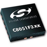
C8051F302 Silicon Laboratories Inc, C8051F302 Datasheet - Page 87

C8051F302
Manufacturer Part Number
C8051F302
Description
IC 8051 MCU 8K FLASH 11MLP
Manufacturer
Silicon Laboratories Inc
Series
C8051F30xr
Specifications of C8051F302
Core Processor
8051
Core Size
8-Bit
Speed
25MHz
Connectivity
SMBus (2-Wire/I²C), UART/USART
Peripherals
POR, PWM, Temp Sensor, WDT
Number Of I /o
8
Program Memory Size
8KB (8K x 8)
Program Memory Type
FLASH
Ram Size
256 x 8
Voltage - Supply (vcc/vdd)
2.7 V ~ 3.6 V
Data Converters
A/D 8x8b
Oscillator Type
External
Operating Temperature
-40°C ~ 85°C
Package / Case
11-VQFN
Data Bus Width
8 bit
Data Ram Size
256 B
Interface Type
I2C, SMBus, UART
Maximum Clock Frequency
25 MHz
Number Of Programmable I/os
8
Number Of Timers
16 bit
Operating Supply Voltage
2.7 V to 3.6 V
Maximum Operating Temperature
+ 85 C
Mounting Style
SMD/SMT
Minimum Operating Temperature
- 40 C
On-chip Adc
8 bit
Lead Free Status / RoHS Status
Contains lead / RoHS non-compliant
Eeprom Size
-
Lead Free Status / Rohs Status
No
Available stocks
Company
Part Number
Manufacturer
Quantity
Price
Company:
Part Number:
C8051F302-GMR
Manufacturer:
SiliconL
Quantity:
3 000
Company:
Part Number:
C8051F302-GMR
Manufacturer:
SILICON
Quantity:
5 000
Part Number:
C8051F302-GMR
Manufacturer:
SILICONLABS/èٹ¯ç§‘
Quantity:
20 000
Bits7-0:
Bits7:
Bits6-0:
FOSE
R/W
R/W
Bit7
Bit7
FLKEY: FLASH Lock and Key Register
Write:
This register must be written to before FLASH writes or erases can be performed. FLASH remains
locked until this register is written to with the following key codes: 0xA5, 0xF1. The timing of the
writes does not matter, as long as the codes are written in order. The key codes must be written for
each FLASH write or erase operation. FLASH will be locked until the next system reset if the wrong
codes are written or if a FLASH operation is attempted before the codes have been written correctly.
Read:
When read, bits 1-0 indicate the current FLASH lock state.
00: FLASH is write/erase locked.
01: The first key code has been written (0xA5).
10: FLASH is unlocked (writes/erases allowed).
11: FLASH writes/erases disabled until the next reset.
FOSE: FLASH One-shot Enable
This bit enables the 50 ns FLASH read one-shot. When the FLASH one-shot disabled, the FLASH
sense amps are enabled for a full clock cycle during FLASH reads.
0: FLASH one-shot disabled.
1: FLASH one-shot enabled.
RESERVED. Read = 0. Must Write 0.
Reserved
R/W
R/W
Bit6
Bit6
Figure 10.3. FLKEY: FLASH Lock and Key Register
Reserved
Figure 10.4. FLSCL: FLASH Scale Register
R/W
R/W
Bit5
Bit5
Reserved
R/W
R/W
Bit4
Bit4
Reserved
R/W
R/W
Bit3
Bit3
Rev. 2.3
Reserved
R/W
R/W
Bit2
Bit2
C8051F300/1/2/3/4/5
Reserved
R/W
R/W
Bit1
Bit1
Reserved
R/W
R/W
Bit0
Bit0
SFR Address:
SFR Address:
00000000
10000000
Reset Value
Reset Value
0xB7
0xB6
87


