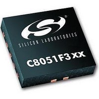
C8051F302 Silicon Laboratories Inc, C8051F302 Datasheet - Page 61

C8051F302
Manufacturer Part Number
C8051F302
Description
IC 8051 MCU 8K FLASH 11MLP
Manufacturer
Silicon Laboratories Inc
Series
C8051F30xr
Specifications of C8051F302
Core Processor
8051
Core Size
8-Bit
Speed
25MHz
Connectivity
SMBus (2-Wire/I²C), UART/USART
Peripherals
POR, PWM, Temp Sensor, WDT
Number Of I /o
8
Program Memory Size
8KB (8K x 8)
Program Memory Type
FLASH
Ram Size
256 x 8
Voltage - Supply (vcc/vdd)
2.7 V ~ 3.6 V
Data Converters
A/D 8x8b
Oscillator Type
External
Operating Temperature
-40°C ~ 85°C
Package / Case
11-VQFN
Data Bus Width
8 bit
Data Ram Size
256 B
Interface Type
I2C, SMBus, UART
Maximum Clock Frequency
25 MHz
Number Of Programmable I/os
8
Number Of Timers
16 bit
Operating Supply Voltage
2.7 V to 3.6 V
Maximum Operating Temperature
+ 85 C
Mounting Style
SMD/SMT
Minimum Operating Temperature
- 40 C
On-chip Adc
8 bit
Lead Free Status / RoHS Status
Contains lead / RoHS non-compliant
Eeprom Size
-
Lead Free Status / Rohs Status
No
Available stocks
Company
Part Number
Manufacturer
Quantity
Price
Company:
Part Number:
C8051F302-GMR
Manufacturer:
SiliconL
Quantity:
3 000
Company:
Part Number:
C8051F302-GMR
Manufacturer:
SILICON
Quantity:
5 000
Part Number:
C8051F302-GMR
Manufacturer:
SILICONLABS/èٹ¯ç§‘
Quantity:
20 000
C8051F300/1/2/3/4/5
The MCS-51™ assembly language allows an alternate notation for bit addressing of the form XX.B where XX is the
byte address and B is the bit position within the byte. For example, the instruction:
MOV
C, 22.3h
moves the Boolean value at 0x13 (bit 3 of the byte at location 0x22) into the Carry flag.
8.2.5. Stack
A programmer's stack can be located anywhere in the 256-byte data memory. The stack area is designated using the
Stack Pointer (SP, 0x81) SFR. The SP will point to the last location used. The next value pushed on the stack is placed
at SP+1 and then SP is incremented. A reset initializes the stack pointer to location 0x07. Therefore, the first value
pushed on the stack is placed at location 0x08, which is also the first register (R0) of register bank 1. Thus, if more
than one register bank is to be used, the SP should be initialized to a location in the data memory not being used for
data storage. The stack depth can extend up to 256 bytes.
8.2.6. Special Function Registers
The direct-access data memory locations from 0x80 to 0xFF constitute the special function registers (SFRs). The
SFRs provide control and data exchange with the CIP-51's resources and peripherals. The CIP-51 duplicates the SFRs
found in a typical 8051 implementation as well as implementing additional SFRs used to configure and access the
sub-systems unique to the MCU. This allows the addition of new functionality while retaining compatibility with the
MCS-51™ instruction set. Table 8.2 lists the SFRs implemented in the CIP-51 System Controller.
The SFR registers are accessed anytime the direct addressing mode is used to access memory locations from 0x80 to
0xFF. SFRs with addresses ending in 0x0 or 0x8 (e.g. P0, TCON, SCON0, IE, etc.) are bit-addressable as well as
byte-addressable. All other SFRs are byte-addressable only. Unoccupied addresses in the SFR space are reserved for
future use. Accessing these areas will have an indeterminate effect and should be avoided. Refer to the corresponding
pages of the datasheet, as indicated in Table 8.3, for a detailed description of each register.
Rev. 2.3
61


