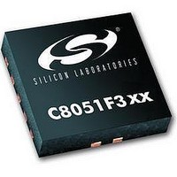
C8051F302 Silicon Laboratories Inc, C8051F302 Datasheet - Page 65

C8051F302
Manufacturer Part Number
C8051F302
Description
IC 8051 MCU 8K FLASH 11MLP
Manufacturer
Silicon Laboratories Inc
Series
C8051F30xr
Specifications of C8051F302
Core Processor
8051
Core Size
8-Bit
Speed
25MHz
Connectivity
SMBus (2-Wire/I²C), UART/USART
Peripherals
POR, PWM, Temp Sensor, WDT
Number Of I /o
8
Program Memory Size
8KB (8K x 8)
Program Memory Type
FLASH
Ram Size
256 x 8
Voltage - Supply (vcc/vdd)
2.7 V ~ 3.6 V
Data Converters
A/D 8x8b
Oscillator Type
External
Operating Temperature
-40°C ~ 85°C
Package / Case
11-VQFN
Data Bus Width
8 bit
Data Ram Size
256 B
Interface Type
I2C, SMBus, UART
Maximum Clock Frequency
25 MHz
Number Of Programmable I/os
8
Number Of Timers
16 bit
Operating Supply Voltage
2.7 V to 3.6 V
Maximum Operating Temperature
+ 85 C
Mounting Style
SMD/SMT
Minimum Operating Temperature
- 40 C
On-chip Adc
8 bit
Lead Free Status / RoHS Status
Contains lead / RoHS non-compliant
Eeprom Size
-
Lead Free Status / Rohs Status
No
Available stocks
Company
Part Number
Manufacturer
Quantity
Price
Company:
Part Number:
C8051F302-GMR
Manufacturer:
SiliconL
Quantity:
3 000
Company:
Part Number:
C8051F302-GMR
Manufacturer:
SILICON
Quantity:
5 000
Part Number:
C8051F302-GMR
Manufacturer:
SILICONLABS/èٹ¯ç§‘
Quantity:
20 000
Bits7-0:
Bit7:
Bit6:
Bit5:
Bits4-3:
Bit2:
Bit1:
Bit0:
R/W
R/W
Bit7
CY
Bit7
SP: Stack Pointer.
The Stack Pointer holds the location of the top of the stack. The stack pointer is incremented before
every PUSH operation. The SP register defaults to 0x07 after reset.
CY: Carry Flag.
This bit is set when the last arithmetic operation resulted in a carry (addition) or a borrow (subtrac-
tion). It is cleared to logic 0 by all other arithmetic operations.
AC: Auxiliary Carry Flag
This bit is set when the last arithmetic operation resulted in a carry into (addition) or a borrow from
(subtraction) the high order nibble. It is cleared to logic 0 by all other arithmetic operations.
F0: User Flag 0.
This is a bit-addressable, general purpose flag for use under software control.
RS1-RS0: Register Bank Select.
These bits select which register bank is used during register accesses.
OV: Overflow Flag.
This bit is set to logic 1 if the last arithmetic operation resulted in a carry (addition), borrow (subtrac-
tion), or overflow (multiply or divide). It is cleared to logic 0 by all other arithmetic operations.
F1: User Flag 1.
This is a bit-addressable, general purpose flag for use under software control.
PARITY: Parity Flag.
This bit is set to logic 1 if the sum of the eight bits in the accumulator is odd and cleared if the sum is
even.
RS1
0
0
1
1
R/W
R/W
AC
Bit6
Bit6
RS0
0
1
0
1
R/W
R/W
Bit5
Bit5
F0
Figure 8.7. PSW: Program Status Word
Register Bank
Figure 8.6. SP: Stack Pointer
RS1
R/W
R/W
Bit4
Bit4
0
1
2
3
RS0
R/W
R/W
Bit3
Bit3
0x08 - 0x0F
0x18 - 0x1F
0x00 - 0x07
0x10 - 0x17
Rev. 2.3
Address
R/W
R/W
OV
Bit2
Bit2
C8051F300/1/2/3/4/5
R/W
R/W
Bit1
Bit1
F1
(bit addressable)
PARITY
R/W
Bit0
Bit0
R
SFR Address:
SFR Address:
00000000
00000111
Reset Value
Reset Value
0xD0
0x81
65


