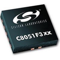
C8051F302 Silicon Laboratories Inc, C8051F302 Datasheet - Page 59

C8051F302
Manufacturer Part Number
C8051F302
Description
IC 8051 MCU 8K FLASH 11MLP
Manufacturer
Silicon Laboratories Inc
Series
C8051F30xr
Specifications of C8051F302
Core Processor
8051
Core Size
8-Bit
Speed
25MHz
Connectivity
SMBus (2-Wire/I²C), UART/USART
Peripherals
POR, PWM, Temp Sensor, WDT
Number Of I /o
8
Program Memory Size
8KB (8K x 8)
Program Memory Type
FLASH
Ram Size
256 x 8
Voltage - Supply (vcc/vdd)
2.7 V ~ 3.6 V
Data Converters
A/D 8x8b
Oscillator Type
External
Operating Temperature
-40°C ~ 85°C
Package / Case
11-VQFN
Data Bus Width
8 bit
Data Ram Size
256 B
Interface Type
I2C, SMBus, UART
Maximum Clock Frequency
25 MHz
Number Of Programmable I/os
8
Number Of Timers
16 bit
Operating Supply Voltage
2.7 V to 3.6 V
Maximum Operating Temperature
+ 85 C
Mounting Style
SMD/SMT
Minimum Operating Temperature
- 40 C
On-chip Adc
8 bit
Lead Free Status / RoHS Status
Contains lead / RoHS non-compliant
Eeprom Size
-
Lead Free Status / Rohs Status
No
Available stocks
Company
Part Number
Manufacturer
Quantity
Price
Company:
Part Number:
C8051F302-GMR
Manufacturer:
SiliconL
Quantity:
3 000
Company:
Part Number:
C8051F302-GMR
Manufacturer:
SILICON
Quantity:
5 000
Part Number:
C8051F302-GMR
Manufacturer:
SILICONLABS/èٹ¯ç§‘
Quantity:
20 000
8.2.
The memory organization of the CIP-51 System Controller is similar to that of a standard 8051. There are two sepa-
rate memory spaces: program memory and data memory. Program and data memory share the same address space but
are accessed via different instruction types. The CIP-51 memory organization is shown in Figure 8.2 and Figure 8.3.
8.2.1. Program Memory
The CIP-51 core has a 64k-byte program memory space. The C8051F300/1/2/3 implements 8192 bytes of this pro-
gram memory space as in-system, re-programmable FLASH memory, organized in a contiguous block from
addresses 0x0000 to 0x1FFF. Note: 512 bytes (0x1E00 - 0x1FFF) of this memory are reserved for factory use and are
not available for user program storage. The C8051F304 implements 4096 bytes of re-programmable FLASH program
memory space; the C8051F305 implements 2048 bytes of re-programmable FLASH program memory space.
Figure 8.2 shows the program memory maps for C8051F300/1/2/3/4/5 devices.
Program memory is normally assumed to be read-only. However, the CIP-51 can write to program memory by setting
the Program Store Write Enable bit (PSCTL.0) and using the MOVX instruction. This feature provides a mechanism
for the CIP-51 to update program code and use the program memory space for non-volatile data storage. Refer to
tion “10. FLASH Memory” on page 83
0x1DFF
0x1E00
0x0000
MEMORY ORGANIZATION
Programmable in 512
C8051F300/1/2/3
(8k FLASH)
Byte Sectors)
RESERVED
(In-System
FLASH
Figure 8.2. Program Memory Maps
for further details.
0x0FFF
0x1000
0x0000
Programmable in 512
(4k FLASH)
C8051F304
Byte Sectors)
RESERVED
(In-System
Rev. 2.3
FLASH
C8051F300/1/2/3/4/5
0x07FF
0x0800
0x0000
Programmable in 512
(2k FLASH)
C8051F305
Byte Sectors)
RESERVED
(In-System
FLASH
Sec-
59


