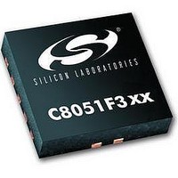
C8051F302 Silicon Laboratories Inc, C8051F302 Datasheet - Page 68

C8051F302
Manufacturer Part Number
C8051F302
Description
IC 8051 MCU 8K FLASH 11MLP
Manufacturer
Silicon Laboratories Inc
Series
C8051F30xr
Specifications of C8051F302
Core Processor
8051
Core Size
8-Bit
Speed
25MHz
Connectivity
SMBus (2-Wire/I²C), UART/USART
Peripherals
POR, PWM, Temp Sensor, WDT
Number Of I /o
8
Program Memory Size
8KB (8K x 8)
Program Memory Type
FLASH
Ram Size
256 x 8
Voltage - Supply (vcc/vdd)
2.7 V ~ 3.6 V
Data Converters
A/D 8x8b
Oscillator Type
External
Operating Temperature
-40°C ~ 85°C
Package / Case
11-VQFN
Data Bus Width
8 bit
Data Ram Size
256 B
Interface Type
I2C, SMBus, UART
Maximum Clock Frequency
25 MHz
Number Of Programmable I/os
8
Number Of Timers
16 bit
Operating Supply Voltage
2.7 V to 3.6 V
Maximum Operating Temperature
+ 85 C
Mounting Style
SMD/SMT
Minimum Operating Temperature
- 40 C
On-chip Adc
8 bit
Lead Free Status / RoHS Status
Contains lead / RoHS non-compliant
Eeprom Size
-
Lead Free Status / Rohs Status
No
Available stocks
Company
Part Number
Manufacturer
Quantity
Price
Company:
Part Number:
C8051F302-GMR
Manufacturer:
SiliconL
Quantity:
3 000
Company:
Part Number:
C8051F302-GMR
Manufacturer:
SILICON
Quantity:
5 000
Part Number:
C8051F302-GMR
Manufacturer:
SILICONLABS/èٹ¯ç§‘
Quantity:
20 000
C8051F300/1/2/3/4/5
8.3.2. External Interrupts
The /INT0 and /INT1 external interrupt sources are configurable as active high or low, edge or level sensitive. The
IN0PL (/INT0 Polarity) and IN1PL (/INT1 Polarity) bits in the IT01CF register select active high or active low; the
IT0 and IT1 bits in TCON
table below lists the possible configurations.
/INT0 and /INT1 are assigned to Port pins as defined in the IT01CF register (see Figure 8.14). Note that /INT0 and
/INT0 Port pin assignments are independent of any Crossbar assignments. /INT0 and /INT1 will monitor their
assigned Port pins without disturbing the peripheral that was assigned the Port pin via the Crossbar. To assign a Port
pin only to /INT0 and/or /INT1, configure the Crossbar to skip the selected pin(s). This is accomplished by setting the
associated bit in register XBR0 (see
configuring the Crossbar).
IE0 (TCON.1) and IE1 (TCON.3) serve as the interrupt-pending flags for the /INT0 and /INT1 external interrupts,
respectively. If an /INT0 or /INT1 external interrupt is configured as edge-sensitive, the corresponding interrupt-
pending flag is automatically cleared by the hardware when the CPU vectors to the ISR. When configured as level
sensitive, the interrupt-pending flag remains logic 1 while the input is active as defined by the corresponding polarity
bit (IN0PL or IN1PL); the flag remains logic 0 while the input is inactive. The external interrupt source must hold the
input active until the interrupt request is recognized. It must then deactivate the interrupt request before execution of
the ISR completes or another interrupt request will be generated.
8.3.3. Interrupt Priorities
Each interrupt source can be individually programmed to one of two priority levels: low or high. A low priority inter-
rupt service routine can be preempted by a high priority interrupt. A high priority interrupt cannot be preempted. Each
interrupt has an associated interrupt priority bit in an SFR (IP or EIP1) used to configure its priority level. Low prior-
ity is the default. If two interrupts are recognized simultaneously, the interrupt with the higher priority is serviced
first. If both interrupts have the same priority level, a fixed priority order is used to arbitrate, given in Table 8.4.
8.3.4. Interrupt Latency
Interrupt response time depends on the state of the CPU when the interrupt occurs. Pending interrupts are sampled
and priority decoded each system clock cycle. Therefore, the fastest possible response time is 5 system clock cycles:
1 clock cycle to detect the interrupt and 4 clock cycles to complete the LCALL to the ISR. If an interrupt is pending
when a RETI is executed, a single instruction is executed before an LCALL is made to service the pending interrupt.
Therefore, the maximum response time for an interrupt (when no other interrupt is currently being serviced or the
new interrupt is of greater priority) occurs when the CPU is performing an RETI instruction followed by a DIV as the
next instruction. In this case, the response time is 18 system clock cycles: 1 clock cycle to detect the interrupt, 5 clock
cycles to execute the RETI, 8 clock cycles to complete the DIV instruction and 4 clock cycles to execute the LCALL
to the ISR. If the CPU is executing an ISR for an interrupt with equal or higher priority, the new interrupt will not be
serviced until the current ISR completes, including the RETI and following instruction.
68
IT0
1
1
0
0
IN0PL
0
1
0
1
/INT0 Interrupt
Active low, edge sensitive
Active high, edge sensitive
Active low, level sensitive
Active high, level sensitive
(Section “15.1. Timer 0 and Timer 1” on page
Section “12.1. Priority Crossbar Decoder” on page 96
Rev. 2.3
IT1
1
1
0
0
133) select level or edge sensitive. The
IN1PL
0
1
0
1
/INT1 Interrupt
Active low, edge sensitive
Active high, edge sensitive
Active low, level sensitive
Active high, level sensitive
for complete details on


