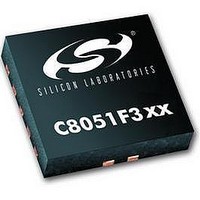
C8051F302 Silicon Laboratories Inc, C8051F302 Datasheet - Page 44

C8051F302
Manufacturer Part Number
C8051F302
Description
IC 8051 MCU 8K FLASH 11MLP
Manufacturer
Silicon Laboratories Inc
Series
C8051F30xr
Specifications of C8051F302
Core Processor
8051
Core Size
8-Bit
Speed
25MHz
Connectivity
SMBus (2-Wire/I²C), UART/USART
Peripherals
POR, PWM, Temp Sensor, WDT
Number Of I /o
8
Program Memory Size
8KB (8K x 8)
Program Memory Type
FLASH
Ram Size
256 x 8
Voltage - Supply (vcc/vdd)
2.7 V ~ 3.6 V
Data Converters
A/D 8x8b
Oscillator Type
External
Operating Temperature
-40°C ~ 85°C
Package / Case
11-VQFN
Data Bus Width
8 bit
Data Ram Size
256 B
Interface Type
I2C, SMBus, UART
Maximum Clock Frequency
25 MHz
Number Of Programmable I/os
8
Number Of Timers
16 bit
Operating Supply Voltage
2.7 V to 3.6 V
Maximum Operating Temperature
+ 85 C
Mounting Style
SMD/SMT
Minimum Operating Temperature
- 40 C
On-chip Adc
8 bit
Lead Free Status / RoHS Status
Contains lead / RoHS non-compliant
Eeprom Size
-
Lead Free Status / Rohs Status
No
Available stocks
Company
Part Number
Manufacturer
Quantity
Price
Company:
Part Number:
C8051F302-GMR
Manufacturer:
SiliconL
Quantity:
3 000
Company:
Part Number:
C8051F302-GMR
Manufacturer:
SILICON
Quantity:
5 000
Part Number:
C8051F302-GMR
Manufacturer:
SILICONLABS/èٹ¯ç§‘
Quantity:
20 000
C8051F300/1/2/3/4/5
44
DC ACCURACY
Resolution
Integral Nonlinearity
Differential Nonlinearity
Offset Error
Full Scale Error
Offset Temperature Coefficient
DYNAMIC PERFORMANCE (10 kHz sine-wave Differential input, 1 dB below Full Scale, 500 ksps)
Signal-to-Noise Plus Distortion
Total Harmonic Distortion
Spurious-Free Dynamic Range
CONVERSION RATE
SAR Conversion Clock
Conversion Time in SAR Clocks
Track/Hold Acquisition Time
Throughput Rate
ANALOG INPUTS
Input Voltage Range
Input Capacitance
TEMPERATURE SENSOR
Linearity
Gain
Offset
POWER SPECIFICATIONS
Power Supply Current (VDD sup-
plied to ADC0)
Power Supply Rejection
Note 1: Represents one standard deviation from the mean.
Note 2: Measured with PGA Gain = 2.
Note 3: Includes ADC offset, gain, and linearity variations.
VDD = 3.0 V, VREF = 2.40 V (REFSL=0), PGA Gain = 1, -40°C to +85°C unless otherwise specified
PARAMETER
Table 5.1. ADC0 Electrical Characteristics
Guaranteed Monotonic
Note 1
Differential mode; See Note 1
Up to the 5
Notes 1, 2, 3
Notes 1, 2, 3
Notes 1, 2, 3 (Temp = 0 °C)
Operating Mode, 500 ksps
CONDITIONS
th
harmonic
Rev. 2.3
MIN
300
45
8
0
0.5±0.6
897±31
-1±0.5
TBD
3350
±110
TYP
±0.5
±0.5
±0.5
±0.3
400
-56
48
58
8
5
VREF
MAX
500
900
±1
±1
6
µV / °C
UNITS
ppm/°C
clocks
mV/V
MHz
LSB
LSB
LSB
LSB
ksps
bits
mV
µA
dB
dB
dB
pF
°C
ns
V


