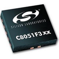
C8051F302 Silicon Laboratories Inc, C8051F302 Datasheet - Page 134

C8051F302
Manufacturer Part Number
C8051F302
Description
IC 8051 MCU 8K FLASH 11MLP
Manufacturer
Silicon Laboratories Inc
Series
C8051F30xr
Specifications of C8051F302
Core Processor
8051
Core Size
8-Bit
Speed
25MHz
Connectivity
SMBus (2-Wire/I²C), UART/USART
Peripherals
POR, PWM, Temp Sensor, WDT
Number Of I /o
8
Program Memory Size
8KB (8K x 8)
Program Memory Type
FLASH
Ram Size
256 x 8
Voltage - Supply (vcc/vdd)
2.7 V ~ 3.6 V
Data Converters
A/D 8x8b
Oscillator Type
External
Operating Temperature
-40°C ~ 85°C
Package / Case
11-VQFN
Data Bus Width
8 bit
Data Ram Size
256 B
Interface Type
I2C, SMBus, UART
Maximum Clock Frequency
25 MHz
Number Of Programmable I/os
8
Number Of Timers
16 bit
Operating Supply Voltage
2.7 V to 3.6 V
Maximum Operating Temperature
+ 85 C
Mounting Style
SMD/SMT
Minimum Operating Temperature
- 40 C
On-chip Adc
8 bit
Lead Free Status / RoHS Status
Contains lead / RoHS non-compliant
Eeprom Size
-
Lead Free Status / Rohs Status
No
Available stocks
Company
Part Number
Manufacturer
Quantity
Price
Company:
Part Number:
C8051F302-GMR
Manufacturer:
SiliconL
Quantity:
3 000
Company:
Part Number:
C8051F302-GMR
Manufacturer:
SILICON
Quantity:
5 000
Part Number:
C8051F302-GMR
Manufacturer:
SILICONLABS/èٹ¯ç§‘
Quantity:
20 000
C8051F300/1/2/3/4/5
Setting the TR0 bit (TCON.4) enables the timer when either GATE0 (TMOD.3) is logic 0 or the input signal /INT0 is
active as defined by bit IN0PL in register INT01CF (see Figure 8.14). Setting GATE0 to ‘1’ allows the timer to be
controlled by the external input signal /INT0 (see
facilitating pulse width measurements.
Setting TR0 does not force the timer to reset. The timer registers should be loaded with the desired initial value before
the timer is enabled.
TL1 and TH1 form the 13-bit register for Timer 1 in the same manner as described above for TL0 and TH0. Timer 1
is configured and controlled using the relevant TCON and TMOD bits just as with Timer 0. The input signal /INT1 is
used with Timer 1; the /INT1 polarity is defined by bit IN1PL in register INT01CF (see Figure 8.14).
15.1.2. Mode 1: 16-bit Counter/Timer
Mode 1 operation is the same as Mode 0, except that the counter/timer registers use all 16 bits. The counter/timers are
enabled and configured in Mode 1 in the same manner as for Mode 0.
134
/INT0
TR0
T0
X = Don't Care
0
1
1
1
Crossbar
GATE0
Pre-scaled Clock
X
0
1
1
SYSCLK
IN0PL
GATE0
/INT0
XOR
X
X
0
1
Figure 15.1. T0 Mode 0 Block Diagram
TR0
0
1
Counter/Timer
M
H
T
2
CKCON
M
T
2
L
Disabled
Disabled
Enabled
Enabled
M
T
1
0
1
M
T
0
Section “8.3.5. Interrupt Register Descriptions” on page
S
C
A
1
S
C
A
Rev. 2.3
0
G
A
T
E
1
C
T
1
/
M
T
1
1
TMOD
M
T
1
0
TCLK
G
A
T
E
0
C
T
0
/
M
T
0
1
M
T
0
0
(5 bits)
TL0
N
1
P
L
I
N
S
1
L
2
I
INT01CF
N
S
1
L
1
I
N
S
1
L
0
I
N
P
0
L
I
(8 bits)
TH0
N
0
S
L
2
I
N
0
S
L
1
I
N
0
S
L
0
I
TR1
TR0
TF1
TF0
IE1
IE0
IT1
IT0
Interrupt
70),


