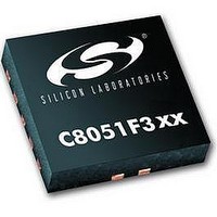
C8051F302 Silicon Laboratories Inc, C8051F302 Datasheet - Page 54

C8051F302
Manufacturer Part Number
C8051F302
Description
IC 8051 MCU 8K FLASH 11MLP
Manufacturer
Silicon Laboratories Inc
Series
C8051F30xr
Specifications of C8051F302
Core Processor
8051
Core Size
8-Bit
Speed
25MHz
Connectivity
SMBus (2-Wire/I²C), UART/USART
Peripherals
POR, PWM, Temp Sensor, WDT
Number Of I /o
8
Program Memory Size
8KB (8K x 8)
Program Memory Type
FLASH
Ram Size
256 x 8
Voltage - Supply (vcc/vdd)
2.7 V ~ 3.6 V
Data Converters
A/D 8x8b
Oscillator Type
External
Operating Temperature
-40°C ~ 85°C
Package / Case
11-VQFN
Data Bus Width
8 bit
Data Ram Size
256 B
Interface Type
I2C, SMBus, UART
Maximum Clock Frequency
25 MHz
Number Of Programmable I/os
8
Number Of Timers
16 bit
Operating Supply Voltage
2.7 V to 3.6 V
Maximum Operating Temperature
+ 85 C
Mounting Style
SMD/SMT
Minimum Operating Temperature
- 40 C
On-chip Adc
8 bit
Lead Free Status / RoHS Status
Contains lead / RoHS non-compliant
Eeprom Size
-
Lead Free Status / Rohs Status
No
Available stocks
Company
Part Number
Manufacturer
Quantity
Price
Company:
Part Number:
C8051F302-GMR
Manufacturer:
SiliconL
Quantity:
3 000
Company:
Part Number:
C8051F302-GMR
Manufacturer:
SILICON
Quantity:
5 000
Part Number:
C8051F302-GMR
Manufacturer:
SILICONLABS/èٹ¯ç§‘
Quantity:
20 000
C8051F300/1/2/3/4/5
Performance
The CIP-51 employs a pipelined architecture that greatly increases its instruction throughput over the standard 8051
architecture. In a standard 8051, all instructions except for MUL and DIV take 12 or 24 system clock cycles to exe-
cute, and usually have a maximum system clock of 12 MHz. By contrast, the CIP-51 core executes 70% of its instruc-
tions in one or two system clock cycles, with no instructions taking more than eight system clock cycles.
With the CIP-51's maximum system clock at 25 MHz, it has a peak throughput of 25 MIPS. The CIP-51 has a total of
109 instructions. The table below shows the total number of instrutions that require each execution time.
Programming and Debugging Support
In-system programming of the FLASH program memory and communication with on-chip debug support logic is
accomplished via the Silicon Labs 2-Wire Development Interface (C2). Note that the re-programmable FLASH can
also be read and changed a single byte at a time by the application software using the MOVC and MOVX instruc-
tions. This feature allows program memory to be used for non-volatile data storage as well as updating program code
under software control.
The on-chip debug support logic facilitates full speed in-circuit debugging, allowing the setting of hardware break-
points, starting, stopping and single stepping through program execution (including interrupt service routines), exam-
ination of the program's call stack, and reading/writing the contents of registers and memory. This method of on-chip
debugging is completely non-intrusive, requiring no RAM, Stack, timers, or other on-chip resources. C2 details can
be found in
The CIP-51 is supported by development tools from Silicon Labs and third party vendors. Silicon Labs provides an
integrated development environment (IDE) including editor, macro assembler, debugger and programmer. The IDE's
debugger and programmer interface to the CIP-51 via the C2 interface to provide fast and efficient in-system device
programming and debugging. Third party macro assemblers and C compilers are also available.
54
Number of Instructions
Clocks to Execute
Section “17. C2 Interface” on page
26
1
50
2
163.
2/3
Rev. 2.3
5
14
3
3/4
7
4
3
4/5
1
5
2
8
1


