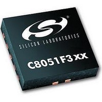
C8051F302 Silicon Laboratories Inc, C8051F302 Datasheet - Page 45

C8051F302
Manufacturer Part Number
C8051F302
Description
IC 8051 MCU 8K FLASH 11MLP
Manufacturer
Silicon Laboratories Inc
Series
C8051F30xr
Specifications of C8051F302
Core Processor
8051
Core Size
8-Bit
Speed
25MHz
Connectivity
SMBus (2-Wire/I²C), UART/USART
Peripherals
POR, PWM, Temp Sensor, WDT
Number Of I /o
8
Program Memory Size
8KB (8K x 8)
Program Memory Type
FLASH
Ram Size
256 x 8
Voltage - Supply (vcc/vdd)
2.7 V ~ 3.6 V
Data Converters
A/D 8x8b
Oscillator Type
External
Operating Temperature
-40°C ~ 85°C
Package / Case
11-VQFN
Data Bus Width
8 bit
Data Ram Size
256 B
Interface Type
I2C, SMBus, UART
Maximum Clock Frequency
25 MHz
Number Of Programmable I/os
8
Number Of Timers
16 bit
Operating Supply Voltage
2.7 V to 3.6 V
Maximum Operating Temperature
+ 85 C
Mounting Style
SMD/SMT
Minimum Operating Temperature
- 40 C
On-chip Adc
8 bit
Lead Free Status / RoHS Status
Contains lead / RoHS non-compliant
Eeprom Size
-
Lead Free Status / Rohs Status
No
Available stocks
Company
Part Number
Manufacturer
Quantity
Price
Company:
Part Number:
C8051F302-GMR
Manufacturer:
SiliconL
Quantity:
3 000
Company:
Part Number:
C8051F302-GMR
Manufacturer:
SILICON
Quantity:
5 000
Part Number:
C8051F302-GMR
Manufacturer:
SILICONLABS/èٹ¯ç§‘
Quantity:
20 000
6.
The voltage reference MUX on C8051F300/2 devices is configurable to use an externally connected voltage refer-
ence or the power supply voltage, VDD (see Figure 6.1). The REFSL bit in the Reference Control register (REF0CN)
selects the reference source. For an external source, REFSL should be set to ‘0’; For VDD as the reference source,
REFSL should be set to ‘1’.
The BIASE bit enables the internal voltage bias generator, which is used by the ADC, Temperature Sensor, and Inter-
nal Oscillator. This bit is forced to logic 1 when any of the aforementioned peripherals is enabled. The bias generator
may be enabled manually by writing a ‘1’ to the BIASE bit in register REF0CN; see Figure 6.2 for REF0CN register
details. The electrical specifications for the voltage reference circuit are given in Table 6.1.
Important Note About the VREF Input: Port pin P0.0 is used as the external VREF input. When using an external
voltage reference, P0.0 should be configured as analog input and skipped by the Digital Crossbar. To configure P0.0
as analog input, set to ‘1’ Bit0 in register P0MDIN. To configure the Crossbar to skip P0.0, set to ‘1’ Bit0 in register
XBR0. Refer to
nal reference voltage must be within the range 0 ≤ VREF ≤ VDD.
On C8051F300/2 devices, the temperature sensor connects to the highest order input of the ADC0 positive input mul-
tiplexer (see
REF0CN enables/disables the temperature sensor. While disabled, the temperature sensor defaults to a high imped-
ance state and any ADC0 measurements performed on the sensor result in meaningless data.
VDD
GND
VOLTAGE REFERENCE (C8051F300/2)
R1
Section “5.1. Analog Multiplexer and PGA” on page 32
Reference
Section “12. Port Input/Output” on page 95
External
Voltage
Circuit
Figure 6.1. Voltage Reference Functional Block Diagram
VREF
VDD
REF0CN
0
1
IOSCEN
Rev. 2.3
for complete Port I/O configuration details. The exter-
EN
EN
Bias Generator
C8051F300/1/2/3/4/5
Temp Sensor
for details). The TEMPE bit in register
To Analog Mux
Internal
VREF
(to ADC)
To ADC, Internal
Oscillator,
Temperature Sensor
45


