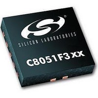
C8051F302 Silicon Laboratories Inc, C8051F302 Datasheet - Page 39

C8051F302
Manufacturer Part Number
C8051F302
Description
IC 8051 MCU 8K FLASH 11MLP
Manufacturer
Silicon Laboratories Inc
Series
C8051F30xr
Specifications of C8051F302
Core Processor
8051
Core Size
8-Bit
Speed
25MHz
Connectivity
SMBus (2-Wire/I²C), UART/USART
Peripherals
POR, PWM, Temp Sensor, WDT
Number Of I /o
8
Program Memory Size
8KB (8K x 8)
Program Memory Type
FLASH
Ram Size
256 x 8
Voltage - Supply (vcc/vdd)
2.7 V ~ 3.6 V
Data Converters
A/D 8x8b
Oscillator Type
External
Operating Temperature
-40°C ~ 85°C
Package / Case
11-VQFN
Data Bus Width
8 bit
Data Ram Size
256 B
Interface Type
I2C, SMBus, UART
Maximum Clock Frequency
25 MHz
Number Of Programmable I/os
8
Number Of Timers
16 bit
Operating Supply Voltage
2.7 V to 3.6 V
Maximum Operating Temperature
+ 85 C
Mounting Style
SMD/SMT
Minimum Operating Temperature
- 40 C
On-chip Adc
8 bit
Lead Free Status / RoHS Status
Contains lead / RoHS non-compliant
Eeprom Size
-
Lead Free Status / Rohs Status
No
Available stocks
Company
Part Number
Manufacturer
Quantity
Price
Company:
Part Number:
C8051F302-GMR
Manufacturer:
SiliconL
Quantity:
3 000
Company:
Part Number:
C8051F302-GMR
Manufacturer:
SILICON
Quantity:
5 000
Part Number:
C8051F302-GMR
Manufacturer:
SILICONLABS/èٹ¯ç§‘
Quantity:
20 000
Bits7-3:
Bit2:
Bits1-0:
Bits7-0:
AD0SC4
R/W
R/W
Bit7
Bit7
AD0SC4-0: ADC0 SAR Conversion Clock Period Bits.
SAR Conversion clock is derived from system clock by the following equation, where AD0SC refers
to the 5-bit value held in bits AD0SC4-0. SAR Conversion clock requirements are given in Table 5.1.
UNUSED. Read = 0b; Write = don’t care.
AMP0GN1-0: ADC0 Internal Amplifier Gain (PGA).
00: Gain = 0.5
01: Gain = 1
10: Gain = 2
11: Gain = 4
ADC0 Data Word.
ADC0 holds the output data byte from the last ADC0 conversion. When in Single-ended mode,
ADC0 holds an 8-bit unsigned integer. When in Differential mode, ADC0 holds a 2’s complement
signed 8-bit integer.
AD0SC
Figure 5.7. ADC0CF: ADC0 Configuration Register (C8051F300/2)
AD0SC3
R/W
R/W
Bit6
Bit6
Figure 5.8. ADC0: ADC0 Data Word Register (C8051F300/2)
=
SYSCLK
--------------------- - 1
CLK
AD0SC2
R/W
R/W
Bit5
Bit5
SAR
–
AD0SC1
R/W
R/W
Bit4
Bit4
AD0SC0
R/W
R/W
Bit3
Bit3
Rev. 2.3
R/W
R/W
Bit2
Bit2
-
C8051F300/1/2/3/4/5
AMP0GN1 AMP0GN0 11111000
R/W
R/W
Bit1
Bit1
R/W
R/W
Bit0
Bit0
SFR Address:
SFR Address:
00000000
Reset Value
Reset Value
0xBC
0xBE
39


