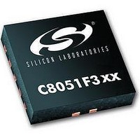
C8051F302 Silicon Laboratories Inc, C8051F302 Datasheet - Page 20

C8051F302
Manufacturer Part Number
C8051F302
Description
IC 8051 MCU 8K FLASH 11MLP
Manufacturer
Silicon Laboratories Inc
Series
C8051F30xr
Specifications of C8051F302
Core Processor
8051
Core Size
8-Bit
Speed
25MHz
Connectivity
SMBus (2-Wire/I²C), UART/USART
Peripherals
POR, PWM, Temp Sensor, WDT
Number Of I /o
8
Program Memory Size
8KB (8K x 8)
Program Memory Type
FLASH
Ram Size
256 x 8
Voltage - Supply (vcc/vdd)
2.7 V ~ 3.6 V
Data Converters
A/D 8x8b
Oscillator Type
External
Operating Temperature
-40°C ~ 85°C
Package / Case
11-VQFN
Data Bus Width
8 bit
Data Ram Size
256 B
Interface Type
I2C, SMBus, UART
Maximum Clock Frequency
25 MHz
Number Of Programmable I/os
8
Number Of Timers
16 bit
Operating Supply Voltage
2.7 V to 3.6 V
Maximum Operating Temperature
+ 85 C
Mounting Style
SMD/SMT
Minimum Operating Temperature
- 40 C
On-chip Adc
8 bit
Lead Free Status / RoHS Status
Contains lead / RoHS non-compliant
Eeprom Size
-
Lead Free Status / Rohs Status
No
Available stocks
Company
Part Number
Manufacturer
Quantity
Price
Company:
Part Number:
C8051F302-GMR
Manufacturer:
SiliconL
Quantity:
3 000
Company:
Part Number:
C8051F302-GMR
Manufacturer:
SILICON
Quantity:
5 000
Part Number:
C8051F302-GMR
Manufacturer:
SILICONLABS/èٹ¯ç§‘
Quantity:
20 000
C8051F300/1/2/3/4/5
1.7.
The C8051F300/2 includes an on-chip 8-bit SAR ADC with a 10-channel differential input multiplexer and program-
mable gain amplifier. With a maximum throughput of 500 ksps, the ADC offers true 8-bit accuracy with an INL of
±1LSB. The ADC system includes a configurable analog multiplexer that selects both positive and negative ADC
inputs. Each Port pin is available as an ADC input; additionally, the on-chip Temperature Sensor output and the
power supply voltage (VDD) are available as ADC inputs. User firmware may shut down the ADC to save power.
The integrated programmable gain amplifier (PGA) amplifies the the ADC input by 0.5, 1, 2, or 4 as defined by user
software. The gain stage is especially useful when different ADC input channels have widely varied input voltage
signals, or when it is necessary to "zoom in" on a signal with a large DC offset.
Conversions can be started in five ways: a software command, an overflow of Timer 0, 1, or 2, or an external convert
start signal. This flexibility allows the start of conversion to be triggered by software events, a periodic signal (timer
overflows), or external HW signals. Conversion completions are indicated by a status bit and an interrupt (if enabled).
The resulting 8-bit data word is latched into an SFR upon completion of a conversion.
Window compare registers for the ADC data can be configured to interrupt the controller when ADC data is either
within or outside of a specified range. The ADC can monitor a key voltage continuously in background mode, but not
interrupt the controller unless the converted data is within/outside the specified range.
20
Sensor
Temp
8-Bit Analog to Digital Converter (C8051F300/2 Only)
DGND
Analog Multiplexer
VDD
P0.0
P0.1
P0.2
P0.3
P0.4
P0.5
P0.6
P0.7
P0.0
P0.1
P0.2
P0.3
P0.4
P0.5
P0.6
P0.7
10-to-1
AMUX
AMUX
9-to-1
Figure 1.9. 8-Bit ADC Block Diagram
Programmable Gain
X
Configuration, Control, and Data Registers
Amplifier
Rev. 2.3
+
-
VDD
ADC
8-Bit
SAR
End of
Conversion
Interrupt
Conversion
Start
Window Compare
8
Logic
Software Write
T0 Overflow
TMR2 Overflow
T1 Overflow
External
Convert Start
ADC Data
Register
Window
Compare
Interrupt


