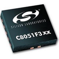
C8051F302 Silicon Laboratories Inc, C8051F302 Datasheet - Page 78

C8051F302
Manufacturer Part Number
C8051F302
Description
IC 8051 MCU 8K FLASH 11MLP
Manufacturer
Silicon Laboratories Inc
Series
C8051F30xr
Specifications of C8051F302
Core Processor
8051
Core Size
8-Bit
Speed
25MHz
Connectivity
SMBus (2-Wire/I²C), UART/USART
Peripherals
POR, PWM, Temp Sensor, WDT
Number Of I /o
8
Program Memory Size
8KB (8K x 8)
Program Memory Type
FLASH
Ram Size
256 x 8
Voltage - Supply (vcc/vdd)
2.7 V ~ 3.6 V
Data Converters
A/D 8x8b
Oscillator Type
External
Operating Temperature
-40°C ~ 85°C
Package / Case
11-VQFN
Data Bus Width
8 bit
Data Ram Size
256 B
Interface Type
I2C, SMBus, UART
Maximum Clock Frequency
25 MHz
Number Of Programmable I/os
8
Number Of Timers
16 bit
Operating Supply Voltage
2.7 V to 3.6 V
Maximum Operating Temperature
+ 85 C
Mounting Style
SMD/SMT
Minimum Operating Temperature
- 40 C
On-chip Adc
8 bit
Lead Free Status / RoHS Status
Contains lead / RoHS non-compliant
Eeprom Size
-
Lead Free Status / Rohs Status
No
Available stocks
Company
Part Number
Manufacturer
Quantity
Price
Company:
Part Number:
C8051F302-GMR
Manufacturer:
SiliconL
Quantity:
3 000
Company:
Part Number:
C8051F302-GMR
Manufacturer:
SILICON
Quantity:
5 000
Part Number:
C8051F302-GMR
Manufacturer:
SILICONLABS/èٹ¯ç§‘
Quantity:
20 000
C8051F300/1/2/3/4/5
9.1.
During power-up, the device is held in a reset state and the /RST pin is driven low until VDD settles above V
delay occurs before the device is released from reset; the delay decreases as the VDD ramp time increases (VDD
ramp time is defined as how fast VDD ramps from 0 V to 2.7 V). Figure 9.2. plots the power-on and VDD monitor
reset timing. The maximum VDD ramp time is 1 ms; slower ramp times may cause the device to be released from
reset before VDD reaches the V
ically less than 0.3 ms.
On exit from a power-on reset, the PORSF flag (RSTSRC.1) is set by hardware to logic 1. When PORSF is set, all of
the other reset flags in the RSTSRC Register are indeterminate (PORSF is cleared by all other resets). Since all resets
cause program execution to begin at the same location (0x0000) software can read the PORSF flag to determine if a
power-up was the cause of reset. The content of internal data memory should be assumed to be undefined after a
power-on reset. The VDD monitor is disabled following a power-on reset.
9.2.
When a power-down transition or power irregularity causes VDD to drop below V
drive the /RST pin low and hold the CIP-51 in a reset state (see Figure 9.2). When VDD returns to a level above
V
altered by the power-fail reset, it is impossible to determine if VDD dropped below the level required for data reten-
tion. If the PORSF flag reads ‘1’, the data may no longer be valid. The VDD monitor is disabled after power-on
resets; however its defined state (enabled/disabled) is not altered by any other reset source. For example, if the VDD
monitor is enabled and a software reset is performed, the VDD monitor will still be enabled after the reset. The VDD
monitor is enabled by writing a ‘1’ to the PORSF bit in register RSTSRC. See Figure 9.2 for VDD monitor timing;
note that the reset delay is not incurred after a VDD monitor reset. See Table 9.2 for electrical characteristics of the
VDD monitor.
78
RST
, the CIP-51 will be released from the reset state. Note that even though internal data memory contents are not
Power-On Reset
Power-Fail Reset / VDD Monitor
Logic HIGH
Logic LOW
2.70
2.55
2.0
1.0
Figure 9.2. Power-On and VDD Monitor Reset Timing
/RST
RST
level. For ramp times less than 1 ms, the power-on reset delay (T
V
RST
Power-On
Reset
T
PORDelay
Rev. 2.3
Monitor
Reset
VDD
RST
, the power supply monitor will
VDD
t
PORDelay
) is typ-
RST
. A


