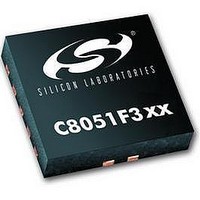
C8051F302 Silicon Laboratories Inc, C8051F302 Datasheet - Page 18

C8051F302
Manufacturer Part Number
C8051F302
Description
IC 8051 MCU 8K FLASH 11MLP
Manufacturer
Silicon Laboratories Inc
Series
C8051F30xr
Specifications of C8051F302
Core Processor
8051
Core Size
8-Bit
Speed
25MHz
Connectivity
SMBus (2-Wire/I²C), UART/USART
Peripherals
POR, PWM, Temp Sensor, WDT
Number Of I /o
8
Program Memory Size
8KB (8K x 8)
Program Memory Type
FLASH
Ram Size
256 x 8
Voltage - Supply (vcc/vdd)
2.7 V ~ 3.6 V
Data Converters
A/D 8x8b
Oscillator Type
External
Operating Temperature
-40°C ~ 85°C
Package / Case
11-VQFN
Data Bus Width
8 bit
Data Ram Size
256 B
Interface Type
I2C, SMBus, UART
Maximum Clock Frequency
25 MHz
Number Of Programmable I/os
8
Number Of Timers
16 bit
Operating Supply Voltage
2.7 V to 3.6 V
Maximum Operating Temperature
+ 85 C
Mounting Style
SMD/SMT
Minimum Operating Temperature
- 40 C
On-chip Adc
8 bit
Lead Free Status / RoHS Status
Contains lead / RoHS non-compliant
Eeprom Size
-
Lead Free Status / Rohs Status
No
Available stocks
Company
Part Number
Manufacturer
Quantity
Price
Company:
Part Number:
C8051F302-GMR
Manufacturer:
SiliconL
Quantity:
3 000
Company:
Part Number:
C8051F302-GMR
Manufacturer:
SILICON
Quantity:
5 000
Part Number:
C8051F302-GMR
Manufacturer:
SILICONLABS/èٹ¯ç§‘
Quantity:
20 000
C8051F300/1/2/3/4/5
1.4.
C8051F300/1/2/3/4/5 devices include a byte-wide I/O Port that behaves like a typical 8051 Port with a few enhance-
ments. Each Port pin may be configured as an analog input or a digital I/O pin. Pins selected as digital I/Os may addi-
tionally be configured for push-pull or open-drain output. The “weak pull-ups” that are fixed on typical 8051 devices
may be globally disabled, providing power savings capabilities.
Perhaps the most unique Port I/O enhancement is the Digital Crossbar. This is essentially a digital switching network
that allows mapping of internal digital system resources to Port I/O pins (See Figure 1.7). On-chip counter/timers,
serial buses, HW interrupts, comparator output, and other digital signals in the controller can be configured to appear
on the Port I/O pins specified in the Crossbar Control registers. This allows the user to select the exact mix of general
purpose Port I/O and digital resources needed for the particular application.
1.5.
The C8051F300/1/2/3/4/5 Family includes an SMBus/I
configuration. Each of the serial buses is fully implemented in hardware and makes extensive use of the CIP-51's
interrupts, thus requiring very little CPU intervention.
18
Highest
Priority
Lowest
Priority
Programmable Digital I/O and Crossbar
Serial Ports
SYSCLK
Outputs
SMBus
T0, T1
UART
CP0
PCA
Port Latch
2
2
2
4
2
Figure 1.7. Digital Crossbar Diagram
P0
(P0.0-P0.7)
8
Rev. 2.3
2
C interface and a full-duplex UART with enhanced baud rate
XBR2 Registers
XBR0, XBR1,
Crossbar
Decoder
Priority
Digital
8
P0MDIN Registers
P0MDOUT,
Cells
I/O
P0
P0.0
P0.7


