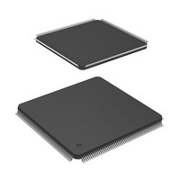
HD6417709SF133B Renesas Electronics America, HD6417709SF133B Datasheet - Page 14

HD6417709SF133B
Manufacturer Part Number
HD6417709SF133B
Description
IC SUPERH MPU ROMLESS 208LQFP
Manufacturer
Renesas Electronics America
Series
SuperH® SH7700r
Datasheet
1.D6417709SBP167BV.pdf
(809 pages)
Specifications of HD6417709SF133B
Core Processor
SH-3
Core Size
32-Bit
Speed
133MHz
Connectivity
EBI/EMI, FIFO, IrDA, SCI, SmartCard
Peripherals
DMA, POR, WDT
Number Of I /o
96
Program Memory Type
ROMless
Ram Size
16K x 8
Voltage - Supply (vcc/vdd)
1.65 V ~ 2.05 V
Data Converters
A/D 8x10b; D/A 2x8b
Oscillator Type
Internal
Operating Temperature
-20°C ~ 75°C
Package / Case
208-LQFP
Lead Free Status / RoHS Status
Contains lead / RoHS non-compliant
Eeprom Size
-
Program Memory Size
-
Available stocks
Company
Part Number
Manufacturer
Quantity
Price
Company:
Part Number:
HD6417709SF133B
Manufacturer:
RENESAS
Quantity:
79
Company:
Part Number:
HD6417709SF133B
Manufacturer:
Renesas Electronics America
Quantity:
10 000
Part Number:
HD6417709SF133B
Manufacturer:
RENESAS/瑞萨
Quantity:
20 000
Part Number:
HD6417709SF133B-V
Manufacturer:
RENESAS/瑞萨
Quantity:
20 000
Part Number:
HD6417709SF133BV
Manufacturer:
RENESAS/瑞萨
Quantity:
20 000
- Current page: 14 of 809
- Download datasheet (5Mb)
Section
10.2.13 MCS0 Control
Register (MCSCR0)
10.3.4 Synchronous
DRAM Interface
10.3.6 PCMCIA
Interface
Figure 10.32 Basic
Timing for PCMCIA
Memory Card Interface
10.3.7 Waits between
Access Cycles
Figure 10.40 Waits
between Access Cycles
10.3.10 MCS[0] to
MCS[7] Pin Control
11.6 Usage Notes
13.4.3 Precautions
when Using RTC
Module Standby
Rev. 5.0, 09/03, page xii of xliv
Page
258
290
310
320
323
387
426
Description
Description added
Bit 6—CS2/CS0 Select (CS2/0)
Only 0 should be used for the CS2/0 bit in MCSCR0. Either 0 or 1
may be used for MCSCR1 to MCSCR7.
Bank Active description added
… .In bank active mode, too, all banks become inactive after a
refresh cycle or after the bus is released as the result of bus
arbitration.
The bank active mode should not be used unless the bus width
for all areas is 32 bits.
Figure amended
D15 to D0
(Write)
Figure amended
CKIO
A25 to A0
Description amended
This enables 32-, 64-, 128-, or 256-Mbit memory to be connected
to area 0 or area 2. However, only CS2/0 = 0 (area 0) should be
used for MCSCR0. Table 10.15 shows MCSCR0–MCSCR7
settings and MCS[0]–MCS[7] assertion conditions.
Description added
13. DMAC transfers should not be performed in the sleep mode
14. When the following three conditions are all met, the
Newly added
under conditions other than when the clock ratio of I (on-
chip clock) to B (bus clock) is 1:1.
frequency control register (FRQCR) should not be changed
while a DMAC transfer is in progress.
Bits IFC2 to IFC0 are changed.
STC2 to STC0 in FRQCR are not changed.
The clock ratio of I (on-chip clock) to B (bus clock) after
the change is other than 1:1.
T
1
T
2
Twait
T
1
T
2
Twait
T
1
T
2
Related parts for HD6417709SF133B
Image
Part Number
Description
Manufacturer
Datasheet
Request
R

Part Number:
Description:
KIT STARTER FOR M16C/29
Manufacturer:
Renesas Electronics America
Datasheet:

Part Number:
Description:
KIT STARTER FOR R8C/2D
Manufacturer:
Renesas Electronics America
Datasheet:

Part Number:
Description:
R0K33062P STARTER KIT
Manufacturer:
Renesas Electronics America
Datasheet:

Part Number:
Description:
KIT STARTER FOR R8C/23 E8A
Manufacturer:
Renesas Electronics America
Datasheet:

Part Number:
Description:
KIT STARTER FOR R8C/25
Manufacturer:
Renesas Electronics America
Datasheet:

Part Number:
Description:
KIT STARTER H8S2456 SHARPE DSPLY
Manufacturer:
Renesas Electronics America
Datasheet:

Part Number:
Description:
KIT STARTER FOR R8C38C
Manufacturer:
Renesas Electronics America
Datasheet:

Part Number:
Description:
KIT STARTER FOR R8C35C
Manufacturer:
Renesas Electronics America
Datasheet:

Part Number:
Description:
KIT STARTER FOR R8CL3AC+LCD APPS
Manufacturer:
Renesas Electronics America
Datasheet:

Part Number:
Description:
KIT STARTER FOR RX610
Manufacturer:
Renesas Electronics America
Datasheet:

Part Number:
Description:
KIT STARTER FOR R32C/118
Manufacturer:
Renesas Electronics America
Datasheet:

Part Number:
Description:
KIT DEV RSK-R8C/26-29
Manufacturer:
Renesas Electronics America
Datasheet:

Part Number:
Description:
KIT STARTER FOR SH7124
Manufacturer:
Renesas Electronics America
Datasheet:

Part Number:
Description:
KIT STARTER FOR H8SX/1622
Manufacturer:
Renesas Electronics America
Datasheet:

Part Number:
Description:
KIT DEV FOR SH7203
Manufacturer:
Renesas Electronics America
Datasheet:


