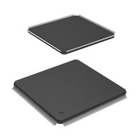
HD6417709SF133B Renesas Electronics America, HD6417709SF133B Datasheet - Page 254

HD6417709SF133B
Manufacturer Part Number
HD6417709SF133B
Description
IC SUPERH MPU ROMLESS 208LQFP
Manufacturer
Renesas Electronics America
Series
SuperH® SH7700r
Datasheet
1.D6417709SBP167BV.pdf
(809 pages)
Specifications of HD6417709SF133B
Core Processor
SH-3
Core Size
32-Bit
Speed
133MHz
Connectivity
EBI/EMI, FIFO, IrDA, SCI, SmartCard
Peripherals
DMA, POR, WDT
Number Of I /o
96
Program Memory Type
ROMless
Ram Size
16K x 8
Voltage - Supply (vcc/vdd)
1.65 V ~ 2.05 V
Data Converters
A/D 8x10b; D/A 2x8b
Oscillator Type
Internal
Operating Temperature
-20°C ~ 75°C
Package / Case
208-LQFP
Lead Free Status / RoHS Status
Contains lead / RoHS non-compliant
Eeprom Size
-
Program Memory Size
-
Available stocks
Company
Part Number
Manufacturer
Quantity
Price
Company:
Part Number:
HD6417709SF133B
Manufacturer:
RENESAS
Quantity:
79
Company:
Part Number:
HD6417709SF133B
Manufacturer:
Renesas Electronics America
Quantity:
10 000
Part Number:
HD6417709SF133B
Manufacturer:
RENESAS/瑞萨
Quantity:
20 000
Part Number:
HD6417709SF133B-V
Manufacturer:
RENESAS/瑞萨
Quantity:
20 000
Part Number:
HD6417709SF133BV
Manufacturer:
RENESAS/瑞萨
Quantity:
20 000
- Current page: 254 of 809
- Download datasheet (5Mb)
Mode 7: In this mode, the CKIO pin is an input, an external clock is input to this pin, and
undergoes waveform shaping, and also frequency multiplication according to the setting, by PLL
circuit 1 before being supplied to the chip. In modes 0 to 2, the system clock is generated from the
output of the chip’s CKIO pin. Consequently, if a large number of ICs are operating on the clock
cycle, the CKIO pin load will be large. This mode, however, assumes a comparatively large-scale
system. If a large number of ICs are operating on the clock cycle, a clock generator with a number
of low-skew clock outputs can be provided, so that the ICs can operate synchronously by
distributing the clocks to each one.
As PLL circuit 1 compensates for fluctuations in the CKIO pin load, this mode is suitable for
connection of synchronous DRAM.
Table 9.4
Clock
Mode FRQCR PLL1
0
Rev. 5.00, 09/03, page 208 of 760
H'0100
H'0101
H'0102
H'0111
H'0112
H'0115
H'0116
H'0122
H'0126
H'012A
H'A100
H'A101
H'E100
H'E101
H'A111
Available Combinations of Clock Mode and FRQCR Values
ON ( 1) ON ( 1) 1:1:1
ON ( 1) ON ( 1) 1:1:1/2
ON ( 1) ON ( 1) 1:1:1/4
ON ( 2) ON ( 1) 2:1:1
ON ( 2) ON ( 1) 2:1:1/2
ON ( 2) ON ( 1) 1:1:1
ON ( 2) ON ( 1) 1:1:1/2
ON ( 4) ON ( 1) 4:1:1
ON ( 4) ON ( 1) 2:1:1
ON ( 4) ON ( 1) 1:1:1
ON ( 3) ON ( 1) 3:1:1
ON ( 3) ON ( 1) 3:1:1/2
ON ( 3) ON ( 1) 1:1:1
ON ( 3) ON ( 1) 1:1:1/2
ON ( 6) ON ( 1) 6:1:1
PLL2
Clock Rate *
(I:B:P)
Input Frequency
Range
25 MHz to 33.34 MHz
25 MHz to 66.67 MHz
25 MHz to 66.67 MHz
25 MHz to 33.34 MHz
25 MHz to 66.67 MHz
25 MHz to 33.34 MHz
25 MHz to 66.67 MHz
25 MHz to 33.34 MHz
25 MHz to 33.34 MHz
25 MHz to 33.34 MHz
25 MHz to 33.34 MHz
25 MHz to 66.67 MHz
25 MHz to 33.34 MHz
25 MHz to 66.67 MHz
25 MHz to 33.34 MHz
CKIO Frequency
Range
25 MHz to 33.34 MHz
25 MHz to 66.67 MHz
25 MHz to 66.67 MHz
25 MHz to 33.34 MHz
25 MHz to 66.67 MHz
25 MHz to 33.34 MHz
25 MHz to 66.67 MHz
25 MHz to 33.34 MHz
25 MHz to 33.34 MHz
25 MHz to 33.34 MHz
25 MHz to 33.34 MHz
25 MHz to 66.67 MHz
25 MHz to 33.34 MHz
25 MHz to 66.67 MHz
25 MHz to 33.34 MHz
Related parts for HD6417709SF133B
Image
Part Number
Description
Manufacturer
Datasheet
Request
R

Part Number:
Description:
KIT STARTER FOR M16C/29
Manufacturer:
Renesas Electronics America
Datasheet:

Part Number:
Description:
KIT STARTER FOR R8C/2D
Manufacturer:
Renesas Electronics America
Datasheet:

Part Number:
Description:
R0K33062P STARTER KIT
Manufacturer:
Renesas Electronics America
Datasheet:

Part Number:
Description:
KIT STARTER FOR R8C/23 E8A
Manufacturer:
Renesas Electronics America
Datasheet:

Part Number:
Description:
KIT STARTER FOR R8C/25
Manufacturer:
Renesas Electronics America
Datasheet:

Part Number:
Description:
KIT STARTER H8S2456 SHARPE DSPLY
Manufacturer:
Renesas Electronics America
Datasheet:

Part Number:
Description:
KIT STARTER FOR R8C38C
Manufacturer:
Renesas Electronics America
Datasheet:

Part Number:
Description:
KIT STARTER FOR R8C35C
Manufacturer:
Renesas Electronics America
Datasheet:

Part Number:
Description:
KIT STARTER FOR R8CL3AC+LCD APPS
Manufacturer:
Renesas Electronics America
Datasheet:

Part Number:
Description:
KIT STARTER FOR RX610
Manufacturer:
Renesas Electronics America
Datasheet:

Part Number:
Description:
KIT STARTER FOR R32C/118
Manufacturer:
Renesas Electronics America
Datasheet:

Part Number:
Description:
KIT DEV RSK-R8C/26-29
Manufacturer:
Renesas Electronics America
Datasheet:

Part Number:
Description:
KIT STARTER FOR SH7124
Manufacturer:
Renesas Electronics America
Datasheet:

Part Number:
Description:
KIT STARTER FOR H8SX/1622
Manufacturer:
Renesas Electronics America
Datasheet:

Part Number:
Description:
KIT DEV FOR SH7203
Manufacturer:
Renesas Electronics America
Datasheet:


