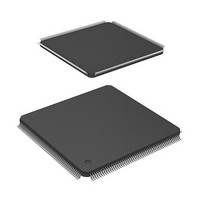
HD6417709SF133B Renesas Electronics America, HD6417709SF133B Datasheet - Page 449

HD6417709SF133B
Manufacturer Part Number
HD6417709SF133B
Description
IC SUPERH MPU ROMLESS 208LQFP
Manufacturer
Renesas Electronics America
Series
SuperH® SH7700r
Datasheet
1.D6417709SBP167BV.pdf
(809 pages)
Specifications of HD6417709SF133B
Core Processor
SH-3
Core Size
32-Bit
Speed
133MHz
Connectivity
EBI/EMI, FIFO, IrDA, SCI, SmartCard
Peripherals
DMA, POR, WDT
Number Of I /o
96
Program Memory Type
ROMless
Ram Size
16K x 8
Voltage - Supply (vcc/vdd)
1.65 V ~ 2.05 V
Data Converters
A/D 8x10b; D/A 2x8b
Oscillator Type
Internal
Operating Temperature
-20°C ~ 75°C
Package / Case
208-LQFP
Lead Free Status / RoHS Status
Contains lead / RoHS non-compliant
Eeprom Size
-
Program Memory Size
-
Available stocks
Company
Part Number
Manufacturer
Quantity
Price
Company:
Part Number:
HD6417709SF133B
Manufacturer:
RENESAS
Quantity:
79
Company:
Part Number:
HD6417709SF133B
Manufacturer:
Renesas Electronics America
Quantity:
10 000
Part Number:
HD6417709SF133B
Manufacturer:
RENESAS/瑞萨
Quantity:
20 000
Part Number:
HD6417709SF133B-V
Manufacturer:
RENESAS/瑞萨
Quantity:
20 000
Part Number:
HD6417709SF133BV
Manufacturer:
RENESAS/瑞萨
Quantity:
20 000
- Current page: 449 of 809
- Download datasheet (5Mb)
12.3.2
Channel 2 has an input capture function (figure 12.7). When using the input capture function, set
the TCLK pin to input mode with the TCOE bit in the timer output control register (TOCR) and
set the timer operation clock to internal clock or on-chip RTC clock with the TPCS2–TPCS0 bits
in the timer control register (TCR2). Also, designate use of the input capture function and whether
to generate interrupts on input capture with the IPCE1–IPCE0 bits in TCR2, and designate the use
of either the rising or falling edge of the TCLK pin to set the timer counter (TCNT2) value into the
input capture register (TCPR2) with the CKEG1–CKEG0 bits in TCR2.
The input capture function cannot be used in standby mode.
pin (TCLK)
clock input
input clock
RTC output
TCNT input
External Clock Operation: Set the TPSC2–TPSC0 bits in TCR to select the external clock
(TCLK) as the timer clock. Use the CKEG1 and CKEG0 bits in TCR to select the detection
edge. Rising, falling, or both edges may be selected. The pulse width of the external clock
must be at least 1.5 peripheral module clock cycles for single edges or 2.5 peripheral module
clock cycles for both edges. A shorter pulse width will result in accurate operation. Figure 12.5
shows the timing for both-edge detection.
On-Chip RTC Clock Operation: Set the TPSC2–TPSC0 bits in TCR to select the on-chip RTC
clock as the timer clock. Figure 12.6 shows the timing.
Figure 12.5 Count Timing when Operating on External Clock (Both Edges Detected)
External
TCNT
TCNT
TCNT
clock
clock
Input Capture Function
P
Figure 12.6 Count Timing when Operating on On-Chip RTC Clock
N + 1
N + 1
N
N
Rev. 5.00, 09/03, page 403 of 760
N
N
1
1
Related parts for HD6417709SF133B
Image
Part Number
Description
Manufacturer
Datasheet
Request
R

Part Number:
Description:
KIT STARTER FOR M16C/29
Manufacturer:
Renesas Electronics America
Datasheet:

Part Number:
Description:
KIT STARTER FOR R8C/2D
Manufacturer:
Renesas Electronics America
Datasheet:

Part Number:
Description:
R0K33062P STARTER KIT
Manufacturer:
Renesas Electronics America
Datasheet:

Part Number:
Description:
KIT STARTER FOR R8C/23 E8A
Manufacturer:
Renesas Electronics America
Datasheet:

Part Number:
Description:
KIT STARTER FOR R8C/25
Manufacturer:
Renesas Electronics America
Datasheet:

Part Number:
Description:
KIT STARTER H8S2456 SHARPE DSPLY
Manufacturer:
Renesas Electronics America
Datasheet:

Part Number:
Description:
KIT STARTER FOR R8C38C
Manufacturer:
Renesas Electronics America
Datasheet:

Part Number:
Description:
KIT STARTER FOR R8C35C
Manufacturer:
Renesas Electronics America
Datasheet:

Part Number:
Description:
KIT STARTER FOR R8CL3AC+LCD APPS
Manufacturer:
Renesas Electronics America
Datasheet:

Part Number:
Description:
KIT STARTER FOR RX610
Manufacturer:
Renesas Electronics America
Datasheet:

Part Number:
Description:
KIT STARTER FOR R32C/118
Manufacturer:
Renesas Electronics America
Datasheet:

Part Number:
Description:
KIT DEV RSK-R8C/26-29
Manufacturer:
Renesas Electronics America
Datasheet:

Part Number:
Description:
KIT STARTER FOR SH7124
Manufacturer:
Renesas Electronics America
Datasheet:

Part Number:
Description:
KIT STARTER FOR H8SX/1622
Manufacturer:
Renesas Electronics America
Datasheet:

Part Number:
Description:
KIT DEV FOR SH7203
Manufacturer:
Renesas Electronics America
Datasheet:


