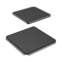
HD6417709SF133B Renesas Electronics America, HD6417709SF133B Datasheet - Page 335

HD6417709SF133B
Manufacturer Part Number
HD6417709SF133B
Description
IC SUPERH MPU ROMLESS 208LQFP
Manufacturer
Renesas Electronics America
Series
SuperH® SH7700r
Datasheet
1.D6417709SBP167BV.pdf
(809 pages)
Specifications of HD6417709SF133B
Core Processor
SH-3
Core Size
32-Bit
Speed
133MHz
Connectivity
EBI/EMI, FIFO, IrDA, SCI, SmartCard
Peripherals
DMA, POR, WDT
Number Of I /o
96
Program Memory Type
ROMless
Ram Size
16K x 8
Voltage - Supply (vcc/vdd)
1.65 V ~ 2.05 V
Data Converters
A/D 8x10b; D/A 2x8b
Oscillator Type
Internal
Operating Temperature
-20°C ~ 75°C
Package / Case
208-LQFP
Lead Free Status / RoHS Status
Contains lead / RoHS non-compliant
Eeprom Size
-
Program Memory Size
-
Available stocks
Company
Part Number
Manufacturer
Quantity
Price
Company:
Part Number:
HD6417709SF133B
Manufacturer:
RENESAS
Quantity:
79
Company:
Part Number:
HD6417709SF133B
Manufacturer:
Renesas Electronics America
Quantity:
10 000
Part Number:
HD6417709SF133B
Manufacturer:
RENESAS/瑞萨
Quantity:
20 000
Part Number:
HD6417709SF133B-V
Manufacturer:
RENESAS/瑞萨
Quantity:
20 000
Part Number:
HD6417709SF133BV
Manufacturer:
RENESAS/瑞萨
Quantity:
20 000
- Current page: 335 of 809
- Download datasheet (5Mb)
Bank Active: The synchronous DRAM bank function is used to support high-speed accesses to
the same row address. When the RASD bit in MCR is 1, read/write command accesses are
performed using commands without auto-precharge (READ, WRIT). In this case, precharging is
not performed when the access ends. When accessing the same row address in the same bank, it is
possible to issue the READ or WRIT command immediately, without issuing an ACTV command,
in the same way as in the RAS down state in DRAM fast page mode. As synchronous DRAM is
internally divided into two or four banks, it is possible to activate one row address in each bank. If
the next access is to a different row address, a PRE command is first issued to precharge the
relevant bank, then when precharging is completed, the access is performed by issuing an ACTV
command followed by a READ or WRIT command. If this is followed by an access to a different
row address, the access time will be longer because of the precharging performed after the access
request is issued.
In a write, when auto-precharge is performed, a command cannot be issued for a period of Trwl +
Tpc cycles after issuance of the WRITA command. When bank active mode is used, READ or
WRIT commands can be issued successively if the row address is the same. The number of cycles
can thus be reduced by Trwl + Tpc cycles for each write. The number of cycles between issuance
of the precharge command and the row address strobe command is determined by the TPC bits in
MCR.
Whether faster execution speed is achieved by use of bank active mode or by use of basic access is
determined by the probability of accessing the same row address (P1), and the average number of
cycles from completion of one access to the next access (Ta). If Ta is greater than Tpc, the delay
due to the precharge wait when writing is imperceptible. In this case, the access speed for bank
active mode and basic access is determined by the number of cycles from the start of access to
issuance of the read/write command: (Tpc + Trcd)
(1 – P1) and Trcd, respectively.
There is a limit on Tras, the time for placing each bank in the active state. If there is no guarantee
that there will not be a cache hit and another row address will be accessed within the period in
which this value is maintained by program execution, it is necessary to set auto-refresh and set the
refresh cycle to no more than the maximum value of Tras. In this way, it is possible to observe the
restrictions on the maximum active state time for each bank. If auto-refresh is not used, measures
must be taken in the program to ensure that the banks do not remain active for longer than the
prescribed time.
A burst read cycle without auto-precharge is shown in figure 10.19, a burst read cycle for the same
row address in figure 10.20, and a burst read cycle for different row addresses in figure 10.21.
Similarly, a burst write cycle without auto-precharge is shown in figure 10.22, a burst write cycle
for the same row address in figure 10.23, and a burst write cycle for different row addresses in
figure 10.24.
Rev. 5.00, 09/03, page 289 of 760
Related parts for HD6417709SF133B
Image
Part Number
Description
Manufacturer
Datasheet
Request
R

Part Number:
Description:
KIT STARTER FOR M16C/29
Manufacturer:
Renesas Electronics America
Datasheet:

Part Number:
Description:
KIT STARTER FOR R8C/2D
Manufacturer:
Renesas Electronics America
Datasheet:

Part Number:
Description:
R0K33062P STARTER KIT
Manufacturer:
Renesas Electronics America
Datasheet:

Part Number:
Description:
KIT STARTER FOR R8C/23 E8A
Manufacturer:
Renesas Electronics America
Datasheet:

Part Number:
Description:
KIT STARTER FOR R8C/25
Manufacturer:
Renesas Electronics America
Datasheet:

Part Number:
Description:
KIT STARTER H8S2456 SHARPE DSPLY
Manufacturer:
Renesas Electronics America
Datasheet:

Part Number:
Description:
KIT STARTER FOR R8C38C
Manufacturer:
Renesas Electronics America
Datasheet:

Part Number:
Description:
KIT STARTER FOR R8C35C
Manufacturer:
Renesas Electronics America
Datasheet:

Part Number:
Description:
KIT STARTER FOR R8CL3AC+LCD APPS
Manufacturer:
Renesas Electronics America
Datasheet:

Part Number:
Description:
KIT STARTER FOR RX610
Manufacturer:
Renesas Electronics America
Datasheet:

Part Number:
Description:
KIT STARTER FOR R32C/118
Manufacturer:
Renesas Electronics America
Datasheet:

Part Number:
Description:
KIT DEV RSK-R8C/26-29
Manufacturer:
Renesas Electronics America
Datasheet:

Part Number:
Description:
KIT STARTER FOR SH7124
Manufacturer:
Renesas Electronics America
Datasheet:

Part Number:
Description:
KIT STARTER FOR H8SX/1622
Manufacturer:
Renesas Electronics America
Datasheet:

Part Number:
Description:
KIT DEV FOR SH7203
Manufacturer:
Renesas Electronics America
Datasheet:


