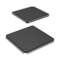
HD6417709SF133B Renesas Electronics America, HD6417709SF133B Datasheet - Page 34

HD6417709SF133B
Manufacturer Part Number
HD6417709SF133B
Description
IC SUPERH MPU ROMLESS 208LQFP
Manufacturer
Renesas Electronics America
Series
SuperH® SH7700r
Datasheet
1.D6417709SBP167BV.pdf
(809 pages)
Specifications of HD6417709SF133B
Core Processor
SH-3
Core Size
32-Bit
Speed
133MHz
Connectivity
EBI/EMI, FIFO, IrDA, SCI, SmartCard
Peripherals
DMA, POR, WDT
Number Of I /o
96
Program Memory Type
ROMless
Ram Size
16K x 8
Voltage - Supply (vcc/vdd)
1.65 V ~ 2.05 V
Data Converters
A/D 8x10b; D/A 2x8b
Oscillator Type
Internal
Operating Temperature
-20°C ~ 75°C
Package / Case
208-LQFP
Lead Free Status / RoHS Status
Contains lead / RoHS non-compliant
Eeprom Size
-
Program Memory Size
-
Available stocks
Company
Part Number
Manufacturer
Quantity
Price
Company:
Part Number:
HD6417709SF133B
Manufacturer:
RENESAS
Quantity:
79
Company:
Part Number:
HD6417709SF133B
Manufacturer:
Renesas Electronics America
Quantity:
10 000
Part Number:
HD6417709SF133B
Manufacturer:
RENESAS/瑞萨
Quantity:
20 000
Part Number:
HD6417709SF133B-V
Manufacturer:
RENESAS/瑞萨
Quantity:
20 000
Part Number:
HD6417709SF133BV
Manufacturer:
RENESAS/瑞萨
Quantity:
20 000
- Current page: 34 of 809
- Download datasheet (5Mb)
Figure 8.3
Figure 8.4
Figure 8.5
Figure 8.6
Figure 8.7
Figure 8.8
Figure 8.9
Figure 8.10
Figure 8.11
Figure 9.1
Figure 9.2
Figure 9.3
Figure 9.4
Figure 9.5
Figure 10.1
Figure 10.2
Figure 10.3
Figure 10.4
Figure 10.5
Figure 10.6
Figure 10.7
Figure 10.8
Figure 10.9
Figure 10.10 Basic Interface Wait Timing (Software Wait Only)............................................. 273
Figure 10.11 Basic Interface Wait State Timing (Wait State Insertion by WAIT Signal
Figure 10.12 Example of 64-Mbit Synchronous DRAM Connection (32-Bit Bus Width)........ 277
Figure 10.13 Example of 64-Mbit Synchronous DRAM Connection (16-Bit Bus Width)........ 278
Figure 10.14 Basic Timing for Synchronous DRAM Burst Read ............................................. 282
Figure 10.15 Synchronous DRAM Burst Read Wait Specification Timing .............................. 283
Figure 10.16 Basic Timing for Synchronous DRAM Single Read............................................ 284
Figure 10.17 Basic Timing for Synchronous DRAM Burst Write ............................................ 286
Figure 10.18 Basic Timing for Synchronous DRAM Single Write........................................... 288
Figure 10.19 Burst Read Timing (No Precharge) ...................................................................... 291
Figure 10.20 Burst Read Timing (Same Row Address) ............................................................ 292
Figure 10.21 Burst Read Timing (Different Row Addresses) ................................................... 293
Figure 10.22 Burst Write Timing (No Precharge) ..................................................................... 294
Figure 10.23 Burst Write Timing (Same Row Address) ........................................................... 295
Figure 10.24 Burst Write Timing (Different Row Addresses) .................................................. 296
Figure 10.25 Auto-Refresh Operation ....................................................................................... 298
Figure 10.26 Synchronous DRAM Auto-Refresh Timing......................................................... 299
Figure 10.27 Synchronous DRAM Self-Refresh Timing .......................................................... 301
Rev. 5.00, 09/03, page xxxii of xliv
Manual Reset STATUS Output............................................................................ 193
Standby to Interrupt STATUS Output.................................................................. 194
Standby to Power-On Reset STATUS Output...................................................... 195
Standby to Manual Reset STATUS Output.......................................................... 196
Sleep to Interrupt STATUS Output ...................................................................... 196
Sleep to Power-On Reset STATUS Output.......................................................... 197
Sleep to Manual Reset STATUS Output.............................................................. 198
Hardware Standby Mode (When CA Goes Low in Normal Operation)............... 200
Hardware Standby Mode Timing (When CA Goes Low during WDT Operation
on Standby Mode Cancellation) ........................................................................... 201
Block Diagram of Clock Pulse Generator ............................................................ 204
Block Diagram of WDT ....................................................................................... 214
Writing to WTCNT and WTCSR......................................................................... 217
Points for Attention when Using Crystal Resonator............................................. 220
Points for Attention when Using PLL Oscillator Circuit ..................................... 221
Block Diagram of Bus State Controller................................................................ 225
Correspondence between Logical Address Space and Physical Address Space .. 229
Physical Space Allocation .................................................................................... 231
PCMCIA Space Allocation .................................................................................. 232
Writing to RFCR, RTCSR, RTCNT, and RTCOR............................................... 257
Basic Timing of Basic Interface ........................................................................... 269
Example of 32-Bit Data-Width Static RAM Connection ..................................... 270
Example of 16-Bit Data-Width Static RAM Connection ..................................... 271
Example of 8-Bit Data-Width Static RAM Connection ....................................... 272
WAITSEL = 1)..................................................................................................... 275
Related parts for HD6417709SF133B
Image
Part Number
Description
Manufacturer
Datasheet
Request
R

Part Number:
Description:
KIT STARTER FOR M16C/29
Manufacturer:
Renesas Electronics America
Datasheet:

Part Number:
Description:
KIT STARTER FOR R8C/2D
Manufacturer:
Renesas Electronics America
Datasheet:

Part Number:
Description:
R0K33062P STARTER KIT
Manufacturer:
Renesas Electronics America
Datasheet:

Part Number:
Description:
KIT STARTER FOR R8C/23 E8A
Manufacturer:
Renesas Electronics America
Datasheet:

Part Number:
Description:
KIT STARTER FOR R8C/25
Manufacturer:
Renesas Electronics America
Datasheet:

Part Number:
Description:
KIT STARTER H8S2456 SHARPE DSPLY
Manufacturer:
Renesas Electronics America
Datasheet:

Part Number:
Description:
KIT STARTER FOR R8C38C
Manufacturer:
Renesas Electronics America
Datasheet:

Part Number:
Description:
KIT STARTER FOR R8C35C
Manufacturer:
Renesas Electronics America
Datasheet:

Part Number:
Description:
KIT STARTER FOR R8CL3AC+LCD APPS
Manufacturer:
Renesas Electronics America
Datasheet:

Part Number:
Description:
KIT STARTER FOR RX610
Manufacturer:
Renesas Electronics America
Datasheet:

Part Number:
Description:
KIT STARTER FOR R32C/118
Manufacturer:
Renesas Electronics America
Datasheet:

Part Number:
Description:
KIT DEV RSK-R8C/26-29
Manufacturer:
Renesas Electronics America
Datasheet:

Part Number:
Description:
KIT STARTER FOR SH7124
Manufacturer:
Renesas Electronics America
Datasheet:

Part Number:
Description:
KIT STARTER FOR H8SX/1622
Manufacturer:
Renesas Electronics America
Datasheet:

Part Number:
Description:
KIT DEV FOR SH7203
Manufacturer:
Renesas Electronics America
Datasheet:


