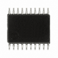
R5F211B1SP#U0 Renesas Electronics America, R5F211B1SP#U0 Datasheet - Page 106

R5F211B1SP#U0
Manufacturer Part Number
R5F211B1SP#U0
Description
IC R8C MCU FLASH 4K 20SSOP
Manufacturer
Renesas Electronics America
Series
M16C™ M16C/R8C/Tiny/1Br
Datasheets
1.R5F211A2SPU0.pdf
(51 pages)
2.R5F211A2SPU0.pdf
(300 pages)
3.R5F211A2SPU0.pdf
(341 pages)
Specifications of R5F211B1SP#U0
Core Processor
R8C
Core Size
16-Bit
Speed
20MHz
Connectivity
I²C, SIO, SSU, UART/USART
Peripherals
LED, POR, Voltage Detect, WDT
Number Of I /o
13
Program Memory Size
4KB (4K x 8)
Program Memory Type
FLASH
Ram Size
384 x 8
Voltage - Supply (vcc/vdd)
2.7 V ~ 5.5 V
Data Converters
A/D 4x10b
Oscillator Type
Internal
Operating Temperature
-20°C ~ 85°C
Package / Case
20-SSOP
For Use With
R0K5211B4S001BE - KIT STARTER FOR R8C/18191A1BR0K5211B4S000BE - KIT DEV EVALUATION R8C/1BR0E521174CPE10 - EMULATOR COMPACT R8C/18/19/1
Lead Free Status / RoHS Status
Lead free / RoHS Compliant
Eeprom Size
-
Available stocks
Company
Part Number
Manufacturer
Quantity
Price
- Current page: 106 of 341
- Download datasheet (4Mb)
R8C/1A Group, R8C/1B Group
Rev.1.30
REJ09B0252-0130
Figure 12.7
Figure 12.8
Address
12.1.6.7
m+1
m
m-4
m-3
m-2
m-1
Stack state before interrupt request
is acknowledged
In the interrupt sequence, the FLG register and PC are saved to the stack.
After an extended 16 bits, 4 high-order bits in the PC and 4 high-order (IPL) and 8 low-order bits in the FLG
register, are saved to the stack, the 16 low-order bits in the PC are saved. Figure 12.7 shows the Stack State
Before and After Acknowledgement of Interrupt Request.
The other necessary registers are saved by a program at the beginning of the interrupt routine. The PUSHM
instruction can save several registers in the register bank being currently used
NOTE:
The register saving operation, which is performed as part of the interrupt sequence, saved in 8 bits at a time in
four steps. Figure 12.8 shows the Register Saving Operation.
MSB
Dec 08, 2006
Previous stack contents
Previous stack contents
1. Selectable from registers R0, R1, R2, R3, A0, A1, SB, and FB.
Address
NOTE :
[SP]−5
[SP]−4
[SP]−3
[SP]−2
[SP]−1
1.[SP] indicates the initial value of the SP when an interrupt request is acknowledged.
NOTE :
[SP]
After registers are saved, the SP content is [SP] minus 4. When executing
software number 32 to 63 INT instructions, this SP is specified by the U
flag. Otherwise it is ISP.
Saving a Register
1.When executing software number 32 to 63 INT instructions,
Stack State Before and After Acknowledgement of Interrupt Request
Register Saving Operation
Stack
this SP is specified by the U flag. Otherwise it is ISP.
FLGH
Page 88 of 315
Stack
LSB
PCM
FLGL
PCL
PCH
[SP]
SP value before
interrupt is generated
Sequence in which
order registers are
saved
Completed saving
registers in four
operations.
(3)
(4)
(1)
(2)
Saved, 8 bits at a time
Address
m+1
m
m-4
m-3
m-2
m-1
Stack state after interrupt request
is acknowledged
MSB
Previous stack contents
Previous stack contents
FLGH
FLGL
PCM
PCL
Stack
PCH
PCM
PCL
FLGH
FLGL
PCH
: 4 high-order bits of PC
: 8 middle-order bits of PC
: 8 low-order bits of PC
: 4 high-order bits of FLG
: 8 low-order bits of FLG
(1)
with a single instruction.
LSB
PCH
PCM : 8 middle-order bits of PC
PCL
FLGH : 4 high-order bits of FLG
FLGL : 8 low-order bits of FLG
[SP]
New SP value
: 4 high-order bits of PC
: 8 low-order bits of PC
12. Interrupts
Related parts for R5F211B1SP#U0
Image
Part Number
Description
Manufacturer
Datasheet
Request
R

Part Number:
Description:
KIT STARTER FOR M16C/29
Manufacturer:
Renesas Electronics America
Datasheet:

Part Number:
Description:
KIT STARTER FOR R8C/2D
Manufacturer:
Renesas Electronics America
Datasheet:

Part Number:
Description:
R0K33062P STARTER KIT
Manufacturer:
Renesas Electronics America
Datasheet:

Part Number:
Description:
KIT STARTER FOR R8C/23 E8A
Manufacturer:
Renesas Electronics America
Datasheet:

Part Number:
Description:
KIT STARTER FOR R8C/25
Manufacturer:
Renesas Electronics America
Datasheet:

Part Number:
Description:
KIT STARTER H8S2456 SHARPE DSPLY
Manufacturer:
Renesas Electronics America
Datasheet:

Part Number:
Description:
KIT STARTER FOR R8C38C
Manufacturer:
Renesas Electronics America
Datasheet:

Part Number:
Description:
KIT STARTER FOR R8C35C
Manufacturer:
Renesas Electronics America
Datasheet:

Part Number:
Description:
KIT STARTER FOR R8CL3AC+LCD APPS
Manufacturer:
Renesas Electronics America
Datasheet:

Part Number:
Description:
KIT STARTER FOR RX610
Manufacturer:
Renesas Electronics America
Datasheet:

Part Number:
Description:
KIT STARTER FOR R32C/118
Manufacturer:
Renesas Electronics America
Datasheet:

Part Number:
Description:
KIT DEV RSK-R8C/26-29
Manufacturer:
Renesas Electronics America
Datasheet:

Part Number:
Description:
KIT STARTER FOR SH7124
Manufacturer:
Renesas Electronics America
Datasheet:

Part Number:
Description:
KIT STARTER FOR H8SX/1622
Manufacturer:
Renesas Electronics America
Datasheet:

Part Number:
Description:
KIT DEV FOR SH7203
Manufacturer:
Renesas Electronics America
Datasheet:


