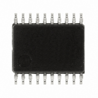
R5F211B1SP#U0 Renesas Electronics America, R5F211B1SP#U0 Datasheet - Page 216

R5F211B1SP#U0
Manufacturer Part Number
R5F211B1SP#U0
Description
IC R8C MCU FLASH 4K 20SSOP
Manufacturer
Renesas Electronics America
Series
M16C™ M16C/R8C/Tiny/1Br
Datasheets
1.R5F211A2SPU0.pdf
(51 pages)
2.R5F211A2SPU0.pdf
(300 pages)
3.R5F211A2SPU0.pdf
(341 pages)
Specifications of R5F211B1SP#U0
Core Processor
R8C
Core Size
16-Bit
Speed
20MHz
Connectivity
I²C, SIO, SSU, UART/USART
Peripherals
LED, POR, Voltage Detect, WDT
Number Of I /o
13
Program Memory Size
4KB (4K x 8)
Program Memory Type
FLASH
Ram Size
384 x 8
Voltage - Supply (vcc/vdd)
2.7 V ~ 5.5 V
Data Converters
A/D 4x10b
Oscillator Type
Internal
Operating Temperature
-20°C ~ 85°C
Package / Case
20-SSOP
For Use With
R0K5211B4S001BE - KIT STARTER FOR R8C/18191A1BR0K5211B4S000BE - KIT DEV EVALUATION R8C/1BR0E521174CPE10 - EMULATOR COMPACT R8C/18/19/1
Lead Free Status / RoHS Status
Lead free / RoHS Compliant
Eeprom Size
-
Available stocks
Company
Part Number
Manufacturer
Quantity
Price
- Current page: 216 of 341
- Download datasheet (4Mb)
R8C/1A Group, R8C/1B Group
Rev.1.30
REJ09B0252-0130
16.2.8
16.2.8.1
16.2.8.2
•
•
•
•
•
•
Set the IICSEL bit in the PMR register to 0 (select clock synchronous serial I/O with chip select function) to use
the clock synchronous serial I/O with chip select function.
After waiting three instructions or more after writing to the registers associated with clock synchronous serial I/
O with chip select (00B8h to 00BFh) or four cycles or more after writing to them, read the registers.
Set the SOOS bit in the SSMR2 register to 0 (CMOS output) in the following settings:
Do not use the SSI01 pin with NMOS open drain output for the above settings.
An example of waiting three instructions or more
An example of waiting four cycles or more
SSUMS bit in SSMR2 register = 1 (4-wire bus communication mode)
BIDE bit in SSMR2 register = 0 (standard mode)
MSS bit in SSCRH register = 0 (operate as slave device)
SSISEL bit in PMR register = 1 (use P1_6 pin for SSI01 pin)
Program example
Program example
Dec 08, 2006
Notes on Clock Synchronous Serial I/O with Chip Select
Accessing Registers Associated with Clock Synchronous Serial I/O
with Chip Select
Selecting SSI Signal Pin
Page 198 of 315
NEXT:
MOV.B
NOP
NOP
NOP
MOV.B
BCLR
JMP.B
BSET
#00h,00BBh
00BBh,R0L
4,00BBh
NEXT
3,00BBh
; Set the SSER register to 00h.
: Disable transmission
: Enable reception
16. Clock Synchronous Serial Interface
Related parts for R5F211B1SP#U0
Image
Part Number
Description
Manufacturer
Datasheet
Request
R

Part Number:
Description:
KIT STARTER FOR M16C/29
Manufacturer:
Renesas Electronics America
Datasheet:

Part Number:
Description:
KIT STARTER FOR R8C/2D
Manufacturer:
Renesas Electronics America
Datasheet:

Part Number:
Description:
R0K33062P STARTER KIT
Manufacturer:
Renesas Electronics America
Datasheet:

Part Number:
Description:
KIT STARTER FOR R8C/23 E8A
Manufacturer:
Renesas Electronics America
Datasheet:

Part Number:
Description:
KIT STARTER FOR R8C/25
Manufacturer:
Renesas Electronics America
Datasheet:

Part Number:
Description:
KIT STARTER H8S2456 SHARPE DSPLY
Manufacturer:
Renesas Electronics America
Datasheet:

Part Number:
Description:
KIT STARTER FOR R8C38C
Manufacturer:
Renesas Electronics America
Datasheet:

Part Number:
Description:
KIT STARTER FOR R8C35C
Manufacturer:
Renesas Electronics America
Datasheet:

Part Number:
Description:
KIT STARTER FOR R8CL3AC+LCD APPS
Manufacturer:
Renesas Electronics America
Datasheet:

Part Number:
Description:
KIT STARTER FOR RX610
Manufacturer:
Renesas Electronics America
Datasheet:

Part Number:
Description:
KIT STARTER FOR R32C/118
Manufacturer:
Renesas Electronics America
Datasheet:

Part Number:
Description:
KIT DEV RSK-R8C/26-29
Manufacturer:
Renesas Electronics America
Datasheet:

Part Number:
Description:
KIT STARTER FOR SH7124
Manufacturer:
Renesas Electronics America
Datasheet:

Part Number:
Description:
KIT STARTER FOR H8SX/1622
Manufacturer:
Renesas Electronics America
Datasheet:

Part Number:
Description:
KIT DEV FOR SH7203
Manufacturer:
Renesas Electronics America
Datasheet:


