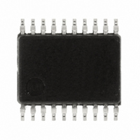
R5F211B1SP#U0 Renesas Electronics America, R5F211B1SP#U0 Datasheet - Page 42

R5F211B1SP#U0
Manufacturer Part Number
R5F211B1SP#U0
Description
IC R8C MCU FLASH 4K 20SSOP
Manufacturer
Renesas Electronics America
Series
M16C™ M16C/R8C/Tiny/1Br
Datasheets
1.R5F211A2SPU0.pdf
(51 pages)
2.R5F211A2SPU0.pdf
(300 pages)
3.R5F211A2SPU0.pdf
(341 pages)
Specifications of R5F211B1SP#U0
Core Processor
R8C
Core Size
16-Bit
Speed
20MHz
Connectivity
I²C, SIO, SSU, UART/USART
Peripherals
LED, POR, Voltage Detect, WDT
Number Of I /o
13
Program Memory Size
4KB (4K x 8)
Program Memory Type
FLASH
Ram Size
384 x 8
Voltage - Supply (vcc/vdd)
2.7 V ~ 5.5 V
Data Converters
A/D 4x10b
Oscillator Type
Internal
Operating Temperature
-20°C ~ 85°C
Package / Case
20-SSOP
For Use With
R0K5211B4S001BE - KIT STARTER FOR R8C/18191A1BR0K5211B4S000BE - KIT DEV EVALUATION R8C/1BR0E521174CPE10 - EMULATOR COMPACT R8C/18/19/1
Lead Free Status / RoHS Status
Lead free / RoHS Compliant
Eeprom Size
-
Available stocks
Company
Part Number
Manufacturer
Quantity
Price
- Current page: 42 of 341
- Download datasheet (4Mb)
R8C/1A Group, R8C/1B Group
Rev.1.30
REJ09B0252-0130
5.
There are 13 programmable Input/Output ports (I/O ports) P1, P3_3 to P3_5, P3_7, and P4_5. 4_2 can be used as an
input-only port. Also, P4_6 and P4_7 can be used as input-only ports if the main clock oscillation circuit is not used.
Table 5.1 lists an Overview of Programmable I/O Ports.
5.1
5.2
5.3
Table 5.1
NOTES:
Table 5.2
NOTE:
Table 5.3
P1
P3_3, P4_5
P3_4, P3_5, P3_7
P4_2, P4_6, P4_7
Reading
Writing
Input
Output
The PDi_j (j=0 to 7) bit in the PDi (i=1, 3, and 4) register controls I/O of ports P1, P3_3 to P3_5, P3_7, and P4_5.
The Pi register consists of a port latch to hold output data and a circuit to read pin states. Figures 5.1 to 5.3 show the
Configurations of Programmable I/O Ports.
Table 5.2 lists the Functions of Programmable I/O Ports. Also, Figure 5.5 shows Registers PD1, PD3, and PD4.
Figure 5.6 shows Registers P1 and P3, Figure 5.9 shows Registers PUR0 and PUR1 and Figure 5.10 shows the
DRR Register.
Programmable I/O ports function as I/O ports for peripheral functions (Refer to Table 1.6 Pin Name Information
by Pin Number of PLSP0020JB-A, PRDP0020BA-A Packages). Table 5.3 lists the Settings of PDi_j Bit when
Functioning as I/O Ports for Peripheral Functions. Refer to the description of each function for information on how
to set peripheral functions.
Figure 5.4 shows the Configuration of I/O Pins.
I/O of Peripheral Functions
Operation when
Programmable I/O Ports
1. In input mode, whether an internal pull-up resistor is connected or not can be selected by registers PUR0 and
2. These ports can be used as the LED drive port by setting the DRR register to 1 (high).
3. When the main clock oscillation circuit is not used, P4_6 and P4_7 can be used as input -only ports.
1. Nothing is assigned to bits PD3_0 to PD3_2, PD3_6, PD4_0 to PD4_4, PD4_6, and PD4_7.
Pi Register
Accessing
PUR1.
Functions of Programmable I/O Ports
Effect on Peripheral Functions
Pins Other than Programmable I/O Ports
Ports
Dec 08, 2006
Overview of Programmable I/O Ports
Functions of Programmable I/O Ports
Settings of PDi_j Bit when Functioning as I/O Ports for Peripheral Functions
(3)
Read pin input level
Write to the port latch
I/O
I/O
I/O
I
When PDi_j Bit is Set to 0 (Input Mode)
I/O
Page 24 of 315
CMOS3 state
CMOS3 state
CMOS3 state
(No output function)
Set this bit to 0 (input mode).
This bit can be set to either 0 or 1 (output regardless of the port setting).
Type of Output
Value of PDi_j Bit in PDi Register
PDi_j Bit Settings for Shared Pin Functions
Set per bit
Set per bit
Set per bit
None
I/O Setting
Read the port latch
Write to the port latch. The value written to the
port latch is output from the pin.
When PDi_j Bit is Set to 1 (Output Mode)
Set every 4 bits
Set every bit
Set every 3 bits
None
Internal Pull-Up
Resistor
(1)
(1)
5. Programmable I/O Ports
(1)
(1)
Set every bit
P1_0 to P1_3
None
None
None
Drive Capacity
Selection
(2)
of
Related parts for R5F211B1SP#U0
Image
Part Number
Description
Manufacturer
Datasheet
Request
R

Part Number:
Description:
KIT STARTER FOR M16C/29
Manufacturer:
Renesas Electronics America
Datasheet:

Part Number:
Description:
KIT STARTER FOR R8C/2D
Manufacturer:
Renesas Electronics America
Datasheet:

Part Number:
Description:
R0K33062P STARTER KIT
Manufacturer:
Renesas Electronics America
Datasheet:

Part Number:
Description:
KIT STARTER FOR R8C/23 E8A
Manufacturer:
Renesas Electronics America
Datasheet:

Part Number:
Description:
KIT STARTER FOR R8C/25
Manufacturer:
Renesas Electronics America
Datasheet:

Part Number:
Description:
KIT STARTER H8S2456 SHARPE DSPLY
Manufacturer:
Renesas Electronics America
Datasheet:

Part Number:
Description:
KIT STARTER FOR R8C38C
Manufacturer:
Renesas Electronics America
Datasheet:

Part Number:
Description:
KIT STARTER FOR R8C35C
Manufacturer:
Renesas Electronics America
Datasheet:

Part Number:
Description:
KIT STARTER FOR R8CL3AC+LCD APPS
Manufacturer:
Renesas Electronics America
Datasheet:

Part Number:
Description:
KIT STARTER FOR RX610
Manufacturer:
Renesas Electronics America
Datasheet:

Part Number:
Description:
KIT STARTER FOR R32C/118
Manufacturer:
Renesas Electronics America
Datasheet:

Part Number:
Description:
KIT DEV RSK-R8C/26-29
Manufacturer:
Renesas Electronics America
Datasheet:

Part Number:
Description:
KIT STARTER FOR SH7124
Manufacturer:
Renesas Electronics America
Datasheet:

Part Number:
Description:
KIT STARTER FOR H8SX/1622
Manufacturer:
Renesas Electronics America
Datasheet:

Part Number:
Description:
KIT DEV FOR SH7203
Manufacturer:
Renesas Electronics America
Datasheet:


