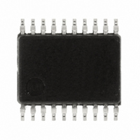
R5F211B1SP#U0 Renesas Electronics America, R5F211B1SP#U0 Datasheet - Page 263

R5F211B1SP#U0
Manufacturer Part Number
R5F211B1SP#U0
Description
IC R8C MCU FLASH 4K 20SSOP
Manufacturer
Renesas Electronics America
Series
M16C™ M16C/R8C/Tiny/1Br
Datasheets
1.R5F211A2SPU0.pdf
(51 pages)
2.R5F211A2SPU0.pdf
(300 pages)
3.R5F211A2SPU0.pdf
(341 pages)
Specifications of R5F211B1SP#U0
Core Processor
R8C
Core Size
16-Bit
Speed
20MHz
Connectivity
I²C, SIO, SSU, UART/USART
Peripherals
LED, POR, Voltage Detect, WDT
Number Of I /o
13
Program Memory Size
4KB (4K x 8)
Program Memory Type
FLASH
Ram Size
384 x 8
Voltage - Supply (vcc/vdd)
2.7 V ~ 5.5 V
Data Converters
A/D 4x10b
Oscillator Type
Internal
Operating Temperature
-20°C ~ 85°C
Package / Case
20-SSOP
For Use With
R0K5211B4S001BE - KIT STARTER FOR R8C/18191A1BR0K5211B4S000BE - KIT DEV EVALUATION R8C/1BR0E521174CPE10 - EMULATOR COMPACT R8C/18/19/1
Lead Free Status / RoHS Status
Lead free / RoHS Compliant
Eeprom Size
-
Available stocks
Company
Part Number
Manufacturer
Quantity
Price
- Current page: 263 of 341
- Download datasheet (4Mb)
R8C/1A Group, R8C/1B Group
Rev.1.30
REJ09B0252-0130
18. Flash Memory
18.1
Table 18.1
NOTES:
Flash memory operating mode
Division of erase block
Programming method
Erase method
Programming and erasure
control method
Rewrite control method
Number of commands
Programming
and erasure
endurance
ID code check function
ROM code protect
In the flash memory, rewrite operations to the flash memory can be performed in three modes; CPU rewrite,
standard serial I/O, and parallel I/O.
Table 18.1 lists the Flash Memory Performance (refer to Table 1.1 Functions and Specifications for R8C/1A
Group and Table 1.2 Functions and Specifications for R8C/1B Group for items not listed in Table 18.1).
1. Definition of programming and erasure endurance
2. Blocks A and B are implemented only in the R8C/1B Group.
The programming and erasure endurance is defined on a per-block basis. If the programming and
erasure endurance is n (n = 100 or 10,000), each block can be erased n times. For example, if 1,024
1-byte writes are performed to block A, a 1-Kbyte block, and then the block is erased, the erase
count stands at one. When performing 100 or more rewrites, the actual erase count can be reduced
by executing programming operations in such a way that all blank areas are used before performing
an erase operation. Avoid rewriting only particular blocks and try to average out the programming
and erasure endurance of the blocks. It is also advisable to retain data on the erase count of each
block and limit the number of erase operations to a certain number.
Overview
Dec 08, 2006
(1)
Flash Memory Performance
Item
Blocks 0 and 1
(program ROM)
Blocks A and B
(data flash)
Page 245 of 315
(2)
3 modes (CPU rewrite, standard serial I/O, and parallel I/O mode)
Refer to Figure 18.1 and Figure 18.2
Byte unit
Block erase
Program and erase control by software command
Rewrite control for blocks 0 and 1 by FMR02 bit in FMR0 register.
Rewrite control for block 0 by FMR15 bit and block 1 by FMR16 bit in
FMR1 register.
5 commands
R8C/1A Group: 100 times; R8C/1B Group: 1,000 times
10,000 times
Standard serial I/O mode supported
Parallel I/O mode supported
Specification
18. Flash Memory
Related parts for R5F211B1SP#U0
Image
Part Number
Description
Manufacturer
Datasheet
Request
R

Part Number:
Description:
KIT STARTER FOR M16C/29
Manufacturer:
Renesas Electronics America
Datasheet:

Part Number:
Description:
KIT STARTER FOR R8C/2D
Manufacturer:
Renesas Electronics America
Datasheet:

Part Number:
Description:
R0K33062P STARTER KIT
Manufacturer:
Renesas Electronics America
Datasheet:

Part Number:
Description:
KIT STARTER FOR R8C/23 E8A
Manufacturer:
Renesas Electronics America
Datasheet:

Part Number:
Description:
KIT STARTER FOR R8C/25
Manufacturer:
Renesas Electronics America
Datasheet:

Part Number:
Description:
KIT STARTER H8S2456 SHARPE DSPLY
Manufacturer:
Renesas Electronics America
Datasheet:

Part Number:
Description:
KIT STARTER FOR R8C38C
Manufacturer:
Renesas Electronics America
Datasheet:

Part Number:
Description:
KIT STARTER FOR R8C35C
Manufacturer:
Renesas Electronics America
Datasheet:

Part Number:
Description:
KIT STARTER FOR R8CL3AC+LCD APPS
Manufacturer:
Renesas Electronics America
Datasheet:

Part Number:
Description:
KIT STARTER FOR RX610
Manufacturer:
Renesas Electronics America
Datasheet:

Part Number:
Description:
KIT STARTER FOR R32C/118
Manufacturer:
Renesas Electronics America
Datasheet:

Part Number:
Description:
KIT DEV RSK-R8C/26-29
Manufacturer:
Renesas Electronics America
Datasheet:

Part Number:
Description:
KIT STARTER FOR SH7124
Manufacturer:
Renesas Electronics America
Datasheet:

Part Number:
Description:
KIT STARTER FOR H8SX/1622
Manufacturer:
Renesas Electronics America
Datasheet:

Part Number:
Description:
KIT DEV FOR SH7203
Manufacturer:
Renesas Electronics America
Datasheet:


