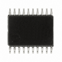
R5F211B1SP#U0 Renesas Electronics America, R5F211B1SP#U0 Datasheet - Page 196

R5F211B1SP#U0
Manufacturer Part Number
R5F211B1SP#U0
Description
IC R8C MCU FLASH 4K 20SSOP
Manufacturer
Renesas Electronics America
Series
M16C™ M16C/R8C/Tiny/1Br
Datasheets
1.R5F211A2SPU0.pdf
(51 pages)
2.R5F211A2SPU0.pdf
(300 pages)
3.R5F211A2SPU0.pdf
(341 pages)
Specifications of R5F211B1SP#U0
Core Processor
R8C
Core Size
16-Bit
Speed
20MHz
Connectivity
I²C, SIO, SSU, UART/USART
Peripherals
LED, POR, Voltage Detect, WDT
Number Of I /o
13
Program Memory Size
4KB (4K x 8)
Program Memory Type
FLASH
Ram Size
384 x 8
Voltage - Supply (vcc/vdd)
2.7 V ~ 5.5 V
Data Converters
A/D 4x10b
Oscillator Type
Internal
Operating Temperature
-20°C ~ 85°C
Package / Case
20-SSOP
For Use With
R0K5211B4S001BE - KIT STARTER FOR R8C/18191A1BR0K5211B4S000BE - KIT DEV EVALUATION R8C/1BR0E521174CPE10 - EMULATOR COMPACT R8C/18/19/1
Lead Free Status / RoHS Status
Lead free / RoHS Compliant
Eeprom Size
-
Available stocks
Company
Part Number
Manufacturer
Quantity
Price
- Current page: 196 of 341
- Download datasheet (4Mb)
R8C/1A Group, R8C/1B Group
Rev.1.30
REJ09B0252-0130
Figure 16.8
Figure 16.9
SS Transmit Data Register
SS Receive Data Register
Port Mode Register
b7 b6
NOTE :
b7 b6 b5 b4 b3 b2 b1 b0
NOTES :
b7 b6 b5 b4 b3 b2
1.
1.
2.
0 0 0
b5 b4
Refer to 16.2.8.1 Accessing Registers Associated w ith Clock Synchronous Serial I/O w ith Chip Select for
more information.
The SSRDR register retains the data received before an overrun error occurs (ORER bit in the SSSR register set to 1
(overrun error)). When an overrun error occurs, the receive data may contain errors and therefore should be
discarded.
Refer to 16.2.8.1 Accessing Registers Associated w ith Clock Synchronous Serial I/O w ith Chip Select for
more information.
Dec 08, 2006
b3
b2
0
PMR Register
Registers SSTDR and SSRDR
b1
b1
0
b0
b0
0
Store the transmit data.
The stored transmit data is transferred to the SSTRSR register and transmission is started
w hen it is detected that the SSTRSR register is empty.
When the next transmit data is w ritten to the SSTDR register during the data transmission from
the SSTRSR register, the data can be transmitted continuously.
When the MLS bit in the SSMR register is set to 1 (transfer data w ith LSB-first), the data in
w hich MSB and LSB are reversed is read, after w riting to the SSTDR register.
Store the receive data.
The receive data is transferred to the SSRDR register and the receive operation is completed
w hen 1 byte of data has been received by the SSTRSR register. At this time, the next receive
operation is possible. Continuous reception is possible using registers SSTRSR and SSRDR.
Bit Symbol
Symbol
SSTDR
Symbol
SSRDR
(b2-b0)
SSISEL
(b6-b4)
Symbol
IICSEL
PMR
Page 178 of 315
—
—
(2)
(1)
Reserved bits
SSI signal pin select bit
Reserved bits
SSU / I
2
C bus sw itch bit
(1)
Address
Bit Name
Address
Address
00F8h
00BEh
00BFh
Function
Function
Set to 0.
0 : P3_3 pin is used for SSI00 pin.
1 : P1_6 pin is used for SSI01 pin.
Set to 0.
0 : Selects SSU function.
1 : Selects I
16. Clock Synchronous Serial Interface
2
C bus function.
After Reset
After Reset
After Reset
Function
00h
FFh
FFh
RW
RW
RW
RW
RW
RW
RW
RW
RO
Related parts for R5F211B1SP#U0
Image
Part Number
Description
Manufacturer
Datasheet
Request
R

Part Number:
Description:
KIT STARTER FOR M16C/29
Manufacturer:
Renesas Electronics America
Datasheet:

Part Number:
Description:
KIT STARTER FOR R8C/2D
Manufacturer:
Renesas Electronics America
Datasheet:

Part Number:
Description:
R0K33062P STARTER KIT
Manufacturer:
Renesas Electronics America
Datasheet:

Part Number:
Description:
KIT STARTER FOR R8C/23 E8A
Manufacturer:
Renesas Electronics America
Datasheet:

Part Number:
Description:
KIT STARTER FOR R8C/25
Manufacturer:
Renesas Electronics America
Datasheet:

Part Number:
Description:
KIT STARTER H8S2456 SHARPE DSPLY
Manufacturer:
Renesas Electronics America
Datasheet:

Part Number:
Description:
KIT STARTER FOR R8C38C
Manufacturer:
Renesas Electronics America
Datasheet:

Part Number:
Description:
KIT STARTER FOR R8C35C
Manufacturer:
Renesas Electronics America
Datasheet:

Part Number:
Description:
KIT STARTER FOR R8CL3AC+LCD APPS
Manufacturer:
Renesas Electronics America
Datasheet:

Part Number:
Description:
KIT STARTER FOR RX610
Manufacturer:
Renesas Electronics America
Datasheet:

Part Number:
Description:
KIT STARTER FOR R32C/118
Manufacturer:
Renesas Electronics America
Datasheet:

Part Number:
Description:
KIT DEV RSK-R8C/26-29
Manufacturer:
Renesas Electronics America
Datasheet:

Part Number:
Description:
KIT STARTER FOR SH7124
Manufacturer:
Renesas Electronics America
Datasheet:

Part Number:
Description:
KIT STARTER FOR H8SX/1622
Manufacturer:
Renesas Electronics America
Datasheet:

Part Number:
Description:
KIT DEV FOR SH7203
Manufacturer:
Renesas Electronics America
Datasheet:


