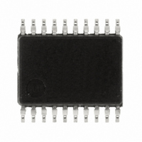
R5F211B1SP#U0 Renesas Electronics America, R5F211B1SP#U0 Datasheet - Page 279

R5F211B1SP#U0
Manufacturer Part Number
R5F211B1SP#U0
Description
IC R8C MCU FLASH 4K 20SSOP
Manufacturer
Renesas Electronics America
Series
M16C™ M16C/R8C/Tiny/1Br
Datasheets
1.R5F211A2SPU0.pdf
(51 pages)
2.R5F211A2SPU0.pdf
(300 pages)
3.R5F211A2SPU0.pdf
(341 pages)
Specifications of R5F211B1SP#U0
Core Processor
R8C
Core Size
16-Bit
Speed
20MHz
Connectivity
I²C, SIO, SSU, UART/USART
Peripherals
LED, POR, Voltage Detect, WDT
Number Of I /o
13
Program Memory Size
4KB (4K x 8)
Program Memory Type
FLASH
Ram Size
384 x 8
Voltage - Supply (vcc/vdd)
2.7 V ~ 5.5 V
Data Converters
A/D 4x10b
Oscillator Type
Internal
Operating Temperature
-20°C ~ 85°C
Package / Case
20-SSOP
For Use With
R0K5211B4S001BE - KIT STARTER FOR R8C/18191A1BR0K5211B4S000BE - KIT DEV EVALUATION R8C/1BR0E521174CPE10 - EMULATOR COMPACT R8C/18/19/1
Lead Free Status / RoHS Status
Lead free / RoHS Compliant
Eeprom Size
-
Available stocks
Company
Part Number
Manufacturer
Quantity
Price
- Current page: 279 of 341
- Download datasheet (4Mb)
R8C/1A Group, R8C/1B Group
Rev.1.30
REJ09B0252-0130
18.4.3
Table 18.4
Read array
Read status register
Clear status register
Program
Block erase
18.4.3.1
18.4.3.2
18.4.3.3
SRD: Status register
WA: Write address (ensure the address specified in the first bus cycle is the same address as the write
WD: Write data (8 bits)
BA: Given block address
×: Any specified address in the user ROM area
The software commands are described below. Read or write commands and data in 8-bit units.
The read array command reads the flash memory.
The MCU enters read array mode when FFh is written in the first bus cycle. When the read address is entered in
the following bus cycles, the content of the specified address can be read in 8-bit units.
Since the MCU remains in read array mode until another command is written, the contents of multiple
addresses can be read continuously.
In addition, the MCU enters read array mode after a reset.
The read status register command is used to read the status register.
When 70h is written in the first bus cycle, the status register can be read in the second bus cycle. (Refer to
18.4.4 Status Register.) When reading the status register, specify an address in the user ROM area.
Do not execute this command in EW1 mode.
The MCU remains in read status register mode until the next read array command is written.
The clear status register command sets the status register to 0.
When 50h is written in the first bus cycle, bits FMR06 to FMR07 in the FMR0 register and SR4 to SR5 in the
status register are set to 0.
Command
address specified in the second bus cycle.)
Dec 08, 2006
Software Commands
Read Array Command
Read Status Register Command
Clear Status Register Command
Software Commands
data (D7 to D0)
Page 261 of 315
Write
Write
Write
Write
Write
Mode
First Bus Cycle
×
×
×
WA
×
Address
FFh
70h
50h
40h
20h
(D7 to D0)
Data
Read
Write
Write
Mode
Second Bus Cycle
×
WA
BA
Address
18. Flash Memory
SRD
WD
D0h
(
D7 to D0)
Data
Related parts for R5F211B1SP#U0
Image
Part Number
Description
Manufacturer
Datasheet
Request
R

Part Number:
Description:
KIT STARTER FOR M16C/29
Manufacturer:
Renesas Electronics America
Datasheet:

Part Number:
Description:
KIT STARTER FOR R8C/2D
Manufacturer:
Renesas Electronics America
Datasheet:

Part Number:
Description:
R0K33062P STARTER KIT
Manufacturer:
Renesas Electronics America
Datasheet:

Part Number:
Description:
KIT STARTER FOR R8C/23 E8A
Manufacturer:
Renesas Electronics America
Datasheet:

Part Number:
Description:
KIT STARTER FOR R8C/25
Manufacturer:
Renesas Electronics America
Datasheet:

Part Number:
Description:
KIT STARTER H8S2456 SHARPE DSPLY
Manufacturer:
Renesas Electronics America
Datasheet:

Part Number:
Description:
KIT STARTER FOR R8C38C
Manufacturer:
Renesas Electronics America
Datasheet:

Part Number:
Description:
KIT STARTER FOR R8C35C
Manufacturer:
Renesas Electronics America
Datasheet:

Part Number:
Description:
KIT STARTER FOR R8CL3AC+LCD APPS
Manufacturer:
Renesas Electronics America
Datasheet:

Part Number:
Description:
KIT STARTER FOR RX610
Manufacturer:
Renesas Electronics America
Datasheet:

Part Number:
Description:
KIT STARTER FOR R32C/118
Manufacturer:
Renesas Electronics America
Datasheet:

Part Number:
Description:
KIT DEV RSK-R8C/26-29
Manufacturer:
Renesas Electronics America
Datasheet:

Part Number:
Description:
KIT STARTER FOR SH7124
Manufacturer:
Renesas Electronics America
Datasheet:

Part Number:
Description:
KIT STARTER FOR H8SX/1622
Manufacturer:
Renesas Electronics America
Datasheet:

Part Number:
Description:
KIT DEV FOR SH7203
Manufacturer:
Renesas Electronics America
Datasheet:


