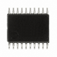
R5F211B1SP#U0 Renesas Electronics America, R5F211B1SP#U0 Datasheet - Page 70

R5F211B1SP#U0
Manufacturer Part Number
R5F211B1SP#U0
Description
IC R8C MCU FLASH 4K 20SSOP
Manufacturer
Renesas Electronics America
Series
M16C™ M16C/R8C/Tiny/1Br
Datasheets
1.R5F211A2SPU0.pdf
(51 pages)
2.R5F211A2SPU0.pdf
(300 pages)
3.R5F211A2SPU0.pdf
(341 pages)
Specifications of R5F211B1SP#U0
Core Processor
R8C
Core Size
16-Bit
Speed
20MHz
Connectivity
I²C, SIO, SSU, UART/USART
Peripherals
LED, POR, Voltage Detect, WDT
Number Of I /o
13
Program Memory Size
4KB (4K x 8)
Program Memory Type
FLASH
Ram Size
384 x 8
Voltage - Supply (vcc/vdd)
2.7 V ~ 5.5 V
Data Converters
A/D 4x10b
Oscillator Type
Internal
Operating Temperature
-20°C ~ 85°C
Package / Case
20-SSOP
For Use With
R0K5211B4S001BE - KIT STARTER FOR R8C/18191A1BR0K5211B4S000BE - KIT DEV EVALUATION R8C/1BR0E521174CPE10 - EMULATOR COMPACT R8C/18/19/1
Lead Free Status / RoHS Status
Lead free / RoHS Compliant
Eeprom Size
-
Available stocks
Company
Part Number
Manufacturer
Quantity
Price
- Current page: 70 of 341
- Download datasheet (4Mb)
R8C/1A Group, R8C/1B Group
Rev.1.30
REJ09B0252-0130
7.2
Figure 7.8
Table 7.2
NOTE:
Table 7.2 lists the Setting Procedure of Voltage Monitor 1 Reset Associated Bits and Figure 7.8 shows an
Operating Example of Voltage Monitor 1 Reset. To use voltage monitor 1 reset to exit stop mode, set the VW1C1
bit in the VW1C register to 1 (digital filter disabled).
1. When the VW1C0 bit is set to 0 (disabled), steps 3, 4, and 5 can be executed simultaneously (with 1
When the VW1C1 bit is set
to 0 (digital filter enabled).
When the VW1C1 bit is set
to 1 (digital filter disabled)
and the VW1C7 bit is set
to 1.
Step
instruction).
3
4
5
Voltage Monitor 1 Reset
1
2
6
7
8
9
(1)
(1)
(1)
VW1C1 and VW1C7: Bits in VW1C Register
Dec 08, 2006
Setting Procedure of Voltage Monitor 1 Reset Associated Bits
Operating Example of Voltage Monitor 1 Reset
Set the VCA26 bit in the VCA2 register to 1 (voltage detection 1 circuit enabled).
Wait for td(E-A)
Select the sampling clock of the digital filter
by bits VW1F0 to VW1F1 in the VW1C
register.
Set the VW1C1 bit in the VW1C register to
0 (digital filter enabled).
Set the VW1C6 bit in the VW1C register to 1 (voltage monitor 1 reset mode).
Set the VW1C2 bit in the VW1C register to 0.
Set the CM14 bit in the CM1 register to 0
(low-speed on-chip oscillator on).
Wait for 4 cycles of the sampling clock of
the digital filter
Set the VW1C0 bit in the VW1C register to 1 (voltage monitor 1 reset enabled).
Internal reset signal
Internal reset signal
The above applies under the following conditions.
• VCA26 bit in VCA2 register = 1 (voltage detection 1 circuit enabled)
• VW1C0 bit in VW1C register = 1 (voltage monitor 1 reset enabled)
• VW1C6 bit in VW1C register = 1 (voltage monitor 1 reset mode)
When the internal reset signal is held “L”, the pins, CPU, and SFR are reset.
The internal reset signal level changes from “L” to “H”, and a program is executed beginning with the address indicated by
the reset vector.
Refer to 4. Special Function Register (SFR) , for the SFR status after reset.
(Typ. 2.85V)
Page 52 of 315
When Using Digital Filter
Vdet1
VCC
Sampling clock of
digital filter x 4 cycles
Set the VW1C7 bit in the VW1C register to
1.
Set the VW1C1 bit in the VW1C register to
1 (digital filter disabled).
−
− (No wait time)
When Not Using Digital Filter
7. Voltage Detection Circuit
fRING-S
fRING-S
1
1
x 32
x 32
Related parts for R5F211B1SP#U0
Image
Part Number
Description
Manufacturer
Datasheet
Request
R

Part Number:
Description:
KIT STARTER FOR M16C/29
Manufacturer:
Renesas Electronics America
Datasheet:

Part Number:
Description:
KIT STARTER FOR R8C/2D
Manufacturer:
Renesas Electronics America
Datasheet:

Part Number:
Description:
R0K33062P STARTER KIT
Manufacturer:
Renesas Electronics America
Datasheet:

Part Number:
Description:
KIT STARTER FOR R8C/23 E8A
Manufacturer:
Renesas Electronics America
Datasheet:

Part Number:
Description:
KIT STARTER FOR R8C/25
Manufacturer:
Renesas Electronics America
Datasheet:

Part Number:
Description:
KIT STARTER H8S2456 SHARPE DSPLY
Manufacturer:
Renesas Electronics America
Datasheet:

Part Number:
Description:
KIT STARTER FOR R8C38C
Manufacturer:
Renesas Electronics America
Datasheet:

Part Number:
Description:
KIT STARTER FOR R8C35C
Manufacturer:
Renesas Electronics America
Datasheet:

Part Number:
Description:
KIT STARTER FOR R8CL3AC+LCD APPS
Manufacturer:
Renesas Electronics America
Datasheet:

Part Number:
Description:
KIT STARTER FOR RX610
Manufacturer:
Renesas Electronics America
Datasheet:

Part Number:
Description:
KIT STARTER FOR R32C/118
Manufacturer:
Renesas Electronics America
Datasheet:

Part Number:
Description:
KIT DEV RSK-R8C/26-29
Manufacturer:
Renesas Electronics America
Datasheet:

Part Number:
Description:
KIT STARTER FOR SH7124
Manufacturer:
Renesas Electronics America
Datasheet:

Part Number:
Description:
KIT STARTER FOR H8SX/1622
Manufacturer:
Renesas Electronics America
Datasheet:

Part Number:
Description:
KIT DEV FOR SH7203
Manufacturer:
Renesas Electronics America
Datasheet:


