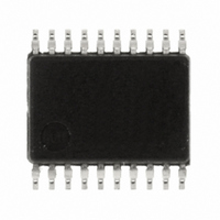
R5F211B1SP#U0 Renesas Electronics America, R5F211B1SP#U0 Datasheet - Page 65

R5F211B1SP#U0
Manufacturer Part Number
R5F211B1SP#U0
Description
IC R8C MCU FLASH 4K 20SSOP
Manufacturer
Renesas Electronics America
Series
M16C™ M16C/R8C/Tiny/1Br
Datasheets
1.R5F211A2SPU0.pdf
(51 pages)
2.R5F211A2SPU0.pdf
(300 pages)
3.R5F211A2SPU0.pdf
(341 pages)
Specifications of R5F211B1SP#U0
Core Processor
R8C
Core Size
16-Bit
Speed
20MHz
Connectivity
I²C, SIO, SSU, UART/USART
Peripherals
LED, POR, Voltage Detect, WDT
Number Of I /o
13
Program Memory Size
4KB (4K x 8)
Program Memory Type
FLASH
Ram Size
384 x 8
Voltage - Supply (vcc/vdd)
2.7 V ~ 5.5 V
Data Converters
A/D 4x10b
Oscillator Type
Internal
Operating Temperature
-20°C ~ 85°C
Package / Case
20-SSOP
For Use With
R0K5211B4S001BE - KIT STARTER FOR R8C/18191A1BR0K5211B4S000BE - KIT DEV EVALUATION R8C/1BR0E521174CPE10 - EMULATOR COMPACT R8C/18/19/1
Lead Free Status / RoHS Status
Lead free / RoHS Compliant
Eeprom Size
-
Available stocks
Company
Part Number
Manufacturer
Quantity
Price
- Current page: 65 of 341
- Download datasheet (4Mb)
R8C/1A Group, R8C/1B Group
Rev.1.30
REJ09B0252-0130
Figure 7.4
Voltage Detection Register 1
Voltage Detection Register 2
b7 b6 b5 b4 b3 b2 b1 b0
NOTES :
b7 b6 b5 b4
NOTES :
0 0 0 0
1.
2.
1.
2.
3.
4.
0 0
The VCA13 bit is enabled w hen the VCA27 bit in the VCA2 register is set to 1 (voltage detection 2 circuit enabled).
The VCA13 bit is set to 1 (VCC ≥ Vdet 2) w hen the VCA27 bit in the VCA2 register is set to 0 (voltage detection 2
circuit disabled).
The softw are reset, w atchdog timer reset, and voltage monitor 2 reset do not affect this register.
Set the PRC3 bit in the PRCR register to 1 (w rite enable) before w riting to this register.
To use the voltage monitor 1 reset, set the VCA26 bit to 1.
After the VCA26 bit is set to 1 from 0, the voltage detection circuit w aits for td(E-A) to elapse before starting
operation.
To use the voltage monitor 2 interrupt/reset or the VCA13 bit in the VCA1 register, set the VCA27 bit to 1.
After the VCA27 bit is set to 1 from 0, the voltage detection circuit w aits for td(E-A) to elapse before starting
operation.
Softw are reset, w atchdog timer reset, and voltage monitor 2 reset do not affect this register.
Dec 08, 2006
b3 b2 b1 b0
0 0 0 0
0
Registers VCA1 and VCA2
0 0
Bit Symbol
Bit Symbol
(b2-b0)
(b7-b4)
Symbol
VCA13
(b5-b0)
VCA26
VCA27
Symbol
VCA1
VCA2
Page 47 of 315
—
—
—
(1)
Reserved bits
Voltage detection 2 signal monitor
flag
Reserved bits
Reserved bits
Voltage detection 1 enable bit
Voltage detection 2 enable bit
(1)
Address
Bit Name
Address
Bit Name
0031h
0032h
(2)
(3)
Set to 0.
0 : VCC < Vdet2
1 : VCC ≥ Vdet2 or voltage detection 2
Set to 0.
Pow er-on reset, voltage monitor 1 reset :
01000000b
Set to 0.
0 : Voltage detection 1 circuit disabled
1 : Voltage detection 1 circuit enabled
0 : Voltage detection 2 circuit disabled
1 : Voltage detection 2 circuit enabled
circuit disabled
Hardw are reset : 00h
After Reset
After Reset
00001000b
Function
Function
7. Voltage Detection Circuit
(2)
(4)
RW
RW
RW
RO
RW
RW
RW
RW
Related parts for R5F211B1SP#U0
Image
Part Number
Description
Manufacturer
Datasheet
Request
R

Part Number:
Description:
KIT STARTER FOR M16C/29
Manufacturer:
Renesas Electronics America
Datasheet:

Part Number:
Description:
KIT STARTER FOR R8C/2D
Manufacturer:
Renesas Electronics America
Datasheet:

Part Number:
Description:
R0K33062P STARTER KIT
Manufacturer:
Renesas Electronics America
Datasheet:

Part Number:
Description:
KIT STARTER FOR R8C/23 E8A
Manufacturer:
Renesas Electronics America
Datasheet:

Part Number:
Description:
KIT STARTER FOR R8C/25
Manufacturer:
Renesas Electronics America
Datasheet:

Part Number:
Description:
KIT STARTER H8S2456 SHARPE DSPLY
Manufacturer:
Renesas Electronics America
Datasheet:

Part Number:
Description:
KIT STARTER FOR R8C38C
Manufacturer:
Renesas Electronics America
Datasheet:

Part Number:
Description:
KIT STARTER FOR R8C35C
Manufacturer:
Renesas Electronics America
Datasheet:

Part Number:
Description:
KIT STARTER FOR R8CL3AC+LCD APPS
Manufacturer:
Renesas Electronics America
Datasheet:

Part Number:
Description:
KIT STARTER FOR RX610
Manufacturer:
Renesas Electronics America
Datasheet:

Part Number:
Description:
KIT STARTER FOR R32C/118
Manufacturer:
Renesas Electronics America
Datasheet:

Part Number:
Description:
KIT DEV RSK-R8C/26-29
Manufacturer:
Renesas Electronics America
Datasheet:

Part Number:
Description:
KIT STARTER FOR SH7124
Manufacturer:
Renesas Electronics America
Datasheet:

Part Number:
Description:
KIT STARTER FOR H8SX/1622
Manufacturer:
Renesas Electronics America
Datasheet:

Part Number:
Description:
KIT DEV FOR SH7203
Manufacturer:
Renesas Electronics America
Datasheet:


