NNDK-MOD5272-KIT NetBurner Inc, NNDK-MOD5272-KIT Datasheet - Page 125
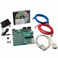
NNDK-MOD5272-KIT
Manufacturer Part Number
NNDK-MOD5272-KIT
Description
KIT DEVELOP NETWORK FOR MOD5272
Manufacturer
NetBurner Inc
Series
ColdFire®r
Datasheets
1.MOD5272-100IR.pdf
(2 pages)
2.MOD5272-100IR.pdf
(550 pages)
3.NNDK-MOD5282-KIT.pdf
(2 pages)
Specifications of NNDK-MOD5272-KIT
Main Purpose
*
Embedded
*
Utilized Ic / Part
MOD5272
Primary Attributes
*
Secondary Attributes
*
Processor To Be Evaluated
MOD5272
Interface Type
RS-232, RS-485, USB
Lead Free Status / RoHS Status
Contains lead / RoHS non-compliant
Lead Free Status / RoHS Status
Lead free / RoHS Compliant, Contains lead / RoHS non-compliant
Other names
528-1001


may not be related to the current bus transfer.
External development systems can use PST outputs with an external image of the program
to completely track the dynamic execution path. This tracking is complicated by any
change in flow, especially when branch target address calculation is based on the contents
of a program-visible register (variant addressing). DDATA outputs can be configured to
display the target address of such instructions in sequential nibble increments across
multiple processor clock cycles, as described in Section 5.3.1, “Begin Execution of Taken
Branch (PST = 0x5).” Two 32-bit storage elements form a FIFO buffer connecting the
processor’s high-speed local bus to the external development system through PST[3:0] and
DDATA[3:0]. The buffer captures branch target addresses and certain data values for
eventual display on the DDATA port, one nibble at a time starting with the least significant
bit (lsb).
Execution speed is affected only when both storage elements contain valid data to be
dumped to the DDATA port. The core stalls until one FIFO entry is available.
Table 5-2 shows the encoding of these signals.
0x8–
MOTOROLA
Hex
0xB
0x0
0x1
0x2
0x3
0x4
0x5
0x6
0x7
PST[3:0]
Binary
1000–
0000
0001
0010
0011
0100
0101
0110
0111
1011
Continue execution. Many instructions execute in one processor cycle. If an instruction requires more
clock cycles, subsequent clock cycles are indicated by driving PST outputs with this encoding.
Begin execution of one instruction. For most instructions, this encoding signals the first clock cycle of
an instruction’s execution. Certain change-of-flow opcodes, plus the PULSE and WDDATA instructions,
generate different encodings.
Reserved
Entry into user-mode. Signaled after execution of the instruction that caused the ColdFire processor to
enter user mode.
Begin execution of PULSE and WDDATA instructions. PULSE defines logic analyzer triggers for debug
and/or performance analysis. WDDATA lets the core write any operand (byte, word, or longword)
directly to the DDATA port, independent of debug module configuration. When WDDATA is executed, a
value of 0x4 is signaled on the PST port, followed by the appropriate marker, and then the data transfer
on the DDATA port. Transfer length depends on the WDDATA operand size.
Begin execution of taken branch. For some opcodes, a branch target address may be displayed on
DDATA depending on the CSR settings. CSR also controls the number of address bytes displayed,
indicated by the PST marker value preceding the DDATA nibble that begins the data output. See
Section 5.3.1, “Begin Execution of Taken Branch (PST = 0x5).”
Reserved
Begin execution of return from exception (RTE) instruction.
Indicates the number of bytes to be displayed on the DDATA port on subsequent clock cycles. The
value is driven onto the PST port one PSTCLK cycle before the data is displayed on DDATA.
0x8 Begin 1-byte transfer on DDATA.
0x9 Begin 2-byte transfer on DDATA.
0xA Begin 3-byte transfer on DDATA.
0xB Begin 4-byte transfer on DDATA.
Table 5-2. Processor Status Encoding
Chapter 5. Debug Support
Definition
Real-Time Trace Support
5-3
Related parts for NNDK-MOD5272-KIT
Image
Part Number
Description
Manufacturer
Datasheet
Request
R

Part Number:
Description:
BOARD SERIAL-ETHERNET 512K FLASH
Manufacturer:
NetBurner Inc
Datasheet:

Part Number:
Description:
PROCESSOR MODULE FLASH MOD5272
Manufacturer:
NetBurner Inc
Datasheet:

Part Number:
Description:
PROCESSOR MODULE 512KB FLASH
Manufacturer:
NetBurner Inc
Datasheet:

Part Number:
Description:
DUAL PORT SERIAL-ETHERNET
Manufacturer:
NetBurner Inc
Datasheet:

Part Number:
Description:
PROCESSOR MODULE FLASH
Manufacturer:
NetBurner Inc
Datasheet:

Part Number:
Description:
PROCESSOR MODULE 512KB FLASH
Manufacturer:
NetBurner Inc
Datasheet:

Part Number:
Description:
MOD5234 10/100 ETHERNET MODULE
Manufacturer:
NetBurner Inc
Datasheet:

Part Number:
Description:
KIT DEVELOP NETWORK FOR MOD5282
Manufacturer:
NetBurner Inc
Datasheet:

Part Number:
Description:
DUAL PORT SERIAL-ETHERNET
Manufacturer:
NetBurner Inc
Datasheet:

Part Number:
Description:
Ethernet Modules & Development Tools 32 Bit 66MHz 40 Pin DIP Industrial Temp
Manufacturer:
NetBurner Inc
Datasheet:

Part Number:
Description:
Ethernet Modules & Development Tools MOD5213 DEVELOPMENT KIT
Manufacturer:
NetBurner Inc

Part Number:
Description:
Ethernet Modules & Development Tools DUAL PORT SERIAL EHTERNET DEVICE
Manufacturer:
NetBurner Inc
Datasheet:

Part Number:
Description:
Ethernet ICs 32bit 147MHz CAN-to- Ethnt Device IndTemp
Manufacturer:
NetBurner Inc
Datasheet: