NNDK-MOD5272-KIT NetBurner Inc, NNDK-MOD5272-KIT Datasheet - Page 398
NNDK-MOD5272-KIT
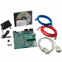
Manufacturer Part Number
NNDK-MOD5272-KIT
Description
KIT DEVELOP NETWORK FOR MOD5272
Manufacturer
NetBurner Inc
Series
ColdFire®r
Datasheets
1.MOD5272-100IR.pdf
(2 pages)
2.MOD5272-100IR.pdf
(550 pages)
3.NNDK-MOD5282-KIT.pdf
(2 pages)
Specifications of NNDK-MOD5272-KIT
Main Purpose
*
Embedded
*
Utilized Ic / Part
MOD5272
Primary Attributes
*
Secondary Attributes
*
Processor To Be Evaluated
MOD5272
Interface Type
RS-232, RS-485, USB
Lead Free Status / RoHS Status
Contains lead / RoHS non-compliant
Lead Free Status / RoHS Status
Lead free / RoHS Compliant, Contains lead / RoHS non-compliant
Other names
528-1001


Port Control Registers
17.2 Port Control Registers
The port control registers are used to configure all pins that carry signals multiplexed from
different on-chip modules. Each pin is configured with a two-bit field. Pin functions are
referred to as function 0b00–0b11. The function 0 signals corresponding to GPIO ports A
and B are immediately available after reset.
Wherever a signal function includes a GPIO port bit, the function defaults to an input after
a reset and can be read in the corresponding port data register.
Pin functions are generally grouped logically. For example, all UART1 signals are
multiplexed with port B and have the control register function code of 0b01.
There is no port C control register. Port C is enabled when the 16-bit-wide external data bus
mode is selected at reset by the input level on QSPI_DOUT/WSEL. The port D control
register is used to configure pins that have multiple functions (0b01 through 0b11) but no
GPIO function.
17.2.1 Port A Control Register (PACNT)
PACNT is used to configure pins that source signals multiplexed with GPIO port A.
17-2
0x0080
0x0084
0x0086
0x0088
0x008C
0x008E
0x0094
0x0096
0x0098
MBAR
Offset
Port C Data Direction Register (PCDDR)
Port B Data Direction Register (PBDDR)
Port A Data Direction Register (PADDR)
Do not attempt to program a pin function that is not defined.
Where no function is defined, the function code is labeled
‘Reserved’ and is considered invalid. Programming any control
register field with a reserved value has an unpredictable effect
on the corresponding pin’s operation.
Reserved function codes cannot be reliably read. Attempts to
read them yield undetermined values.
[31:24]
Table 17-2. GPIO Port Register Memory Map
Reserved
Reserved
Reserved
MCF5272 User’s Manual
[23:16]
Port D Control Register (PDCNT)
Port B Control Register (PBCNT)
Port A Control Register (PACNT)
CAUTION:
[15:8]
Port C Data Register (PCDAT)
Port A Data Register (PADAT)
Port B Data Register (PBDAT)
Reserved
Reserved
Reserved
[7:0]
MOTOROLA
Related parts for NNDK-MOD5272-KIT
Image
Part Number
Description
Manufacturer
Datasheet
Request
R

Part Number:
Description:
BOARD SERIAL-ETHERNET 512K FLASH
Manufacturer:
NetBurner Inc
Datasheet:

Part Number:
Description:
PROCESSOR MODULE FLASH MOD5272
Manufacturer:
NetBurner Inc
Datasheet:

Part Number:
Description:
PROCESSOR MODULE 512KB FLASH
Manufacturer:
NetBurner Inc
Datasheet:

Part Number:
Description:
DUAL PORT SERIAL-ETHERNET
Manufacturer:
NetBurner Inc
Datasheet:

Part Number:
Description:
PROCESSOR MODULE FLASH
Manufacturer:
NetBurner Inc
Datasheet:

Part Number:
Description:
PROCESSOR MODULE 512KB FLASH
Manufacturer:
NetBurner Inc
Datasheet:

Part Number:
Description:
MOD5234 10/100 ETHERNET MODULE
Manufacturer:
NetBurner Inc
Datasheet:

Part Number:
Description:
KIT DEVELOP NETWORK FOR MOD5282
Manufacturer:
NetBurner Inc
Datasheet:

Part Number:
Description:
DUAL PORT SERIAL-ETHERNET
Manufacturer:
NetBurner Inc
Datasheet:

Part Number:
Description:
Ethernet Modules & Development Tools 32 Bit 66MHz 40 Pin DIP Industrial Temp
Manufacturer:
NetBurner Inc
Datasheet:

Part Number:
Description:
Ethernet Modules & Development Tools MOD5213 DEVELOPMENT KIT
Manufacturer:
NetBurner Inc

Part Number:
Description:
Ethernet Modules & Development Tools DUAL PORT SERIAL EHTERNET DEVICE
Manufacturer:
NetBurner Inc
Datasheet:

Part Number:
Description:
Ethernet ICs 32bit 147MHz CAN-to- Ethnt Device IndTemp
Manufacturer:
NetBurner Inc
Datasheet: