NNDK-MOD5272-KIT NetBurner Inc, NNDK-MOD5272-KIT Datasheet - Page 424
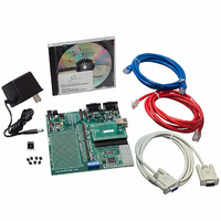
NNDK-MOD5272-KIT
Manufacturer Part Number
NNDK-MOD5272-KIT
Description
KIT DEVELOP NETWORK FOR MOD5272
Manufacturer
NetBurner Inc
Series
ColdFire®r
Datasheets
1.MOD5272-100IR.pdf
(2 pages)
2.MOD5272-100IR.pdf
(550 pages)
3.NNDK-MOD5282-KIT.pdf
(2 pages)
Specifications of NNDK-MOD5272-KIT
Main Purpose
*
Embedded
*
Utilized Ic / Part
MOD5272
Primary Attributes
*
Secondary Attributes
*
Processor To Be Evaluated
MOD5272
Interface Type
RS-232, RS-485, USB
Lead Free Status / RoHS Status
Contains lead / RoHS non-compliant
Lead Free Status / RoHS Status
Lead free / RoHS Compliant, Contains lead / RoHS non-compliant
Other names
528-1001


1
2
3
4
5
(see notes)
Configured
Signal List
Table 19-2 presents signal names, functions, and descriptions sorted by pin numbers.
BGA
No entry in this column means that after reset the pin is not reconfigurable and has only one definition.
WSEL, BUSW1, BUSW0, HIZ, and others, refers to function determined by pull-up or pull-down value as seen by
these address pins during reset.
“Port x Cntl Reg” refers to pin function programmed by software writing to GPIO port configuration registers.
MTMOD means that pin function is determined by state of the MTMOD signal.
Requires external protection circuitry to meet USB 1.1 electrical requirements under all conditions (see 12.5.3,
“Recommended USB Protection Circuit”).
Map
19-10
A10
Pin
A1
A2
A3
A4
A5
A6
A7
A8
A9
by
1
0 (Reset)
DDATA3
DDATA1
RAS0
TEA
BS0
Table 19-1. Signal Descriptions Sorted by Function (Continued)
D16
D18
D21
D22
TDI
USB_GND
USB_VDD
0 (Reset)
USB_D+
USB_D–
VDD
Table 19-2. Signal Name and Description by Pin Number
Pin Functions
DSI
D0
D2
D5
D6
1
–
–
–
–
–
Pin Functions
+3.3V
1
–
–
–
–
MCF5272 User’s Manual
2
–
–
–
–
–
–
–
–
–
–
2
–
–
–
–
3
–
–
–
–
–
–
–
–
–
–
3
–
–
–
–
USB line driver high,
analog
USB line driver low,
analog
USB transceiver GND
USB transceiver VDD
DDATA3
DDATA1
TDI/DSI
D16/D0
D18/D2
D21/D5
D22/D6
Name
RAS0
TEA
BS0
Description
5
5
Debug data 3
Debug data 1
BDM debug transfer
error acknowledge
JTAG test data in/BDM
data in
D16/D0
D18/D2
D21/D5
D22/D6
Byte strobe 0
SDRAM row select
strobe
G[5,10]
H[5,10]
F[9,10]
J[9,10]
F[5,6]
K[7,8]
J[5,6]
BGA
Map
N13
Pin
G2
G1
F1
F2
Description
I/O
O
O
I
I
MOTOROLA
Drive
(mA)
–
–
Cpf
I/O
I/O
I/O
I/O
I/O
30
30
O
O
O
O
I
I
Related parts for NNDK-MOD5272-KIT
Image
Part Number
Description
Manufacturer
Datasheet
Request
R

Part Number:
Description:
BOARD SERIAL-ETHERNET 512K FLASH
Manufacturer:
NetBurner Inc
Datasheet:

Part Number:
Description:
PROCESSOR MODULE FLASH MOD5272
Manufacturer:
NetBurner Inc
Datasheet:

Part Number:
Description:
PROCESSOR MODULE 512KB FLASH
Manufacturer:
NetBurner Inc
Datasheet:

Part Number:
Description:
DUAL PORT SERIAL-ETHERNET
Manufacturer:
NetBurner Inc
Datasheet:

Part Number:
Description:
PROCESSOR MODULE FLASH
Manufacturer:
NetBurner Inc
Datasheet:

Part Number:
Description:
PROCESSOR MODULE 512KB FLASH
Manufacturer:
NetBurner Inc
Datasheet:

Part Number:
Description:
MOD5234 10/100 ETHERNET MODULE
Manufacturer:
NetBurner Inc
Datasheet:

Part Number:
Description:
KIT DEVELOP NETWORK FOR MOD5282
Manufacturer:
NetBurner Inc
Datasheet:

Part Number:
Description:
DUAL PORT SERIAL-ETHERNET
Manufacturer:
NetBurner Inc
Datasheet:

Part Number:
Description:
Ethernet Modules & Development Tools 32 Bit 66MHz 40 Pin DIP Industrial Temp
Manufacturer:
NetBurner Inc
Datasheet:

Part Number:
Description:
Ethernet Modules & Development Tools MOD5213 DEVELOPMENT KIT
Manufacturer:
NetBurner Inc

Part Number:
Description:
Ethernet Modules & Development Tools DUAL PORT SERIAL EHTERNET DEVICE
Manufacturer:
NetBurner Inc
Datasheet:

Part Number:
Description:
Ethernet ICs 32bit 147MHz CAN-to- Ethnt Device IndTemp
Manufacturer:
NetBurner Inc
Datasheet: