NNDK-MOD5272-KIT NetBurner Inc, NNDK-MOD5272-KIT Datasheet - Page 201
NNDK-MOD5272-KIT
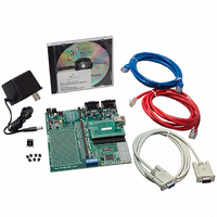
Manufacturer Part Number
NNDK-MOD5272-KIT
Description
KIT DEVELOP NETWORK FOR MOD5272
Manufacturer
NetBurner Inc
Series
ColdFire®r
Datasheets
1.MOD5272-100IR.pdf
(2 pages)
2.MOD5272-100IR.pdf
(550 pages)
3.NNDK-MOD5282-KIT.pdf
(2 pages)
Specifications of NNDK-MOD5272-KIT
Main Purpose
*
Embedded
*
Utilized Ic / Part
MOD5272
Primary Attributes
*
Secondary Attributes
*
Processor To Be Evaluated
MOD5272
Interface Type
RS-232, RS-485, USB
Lead Free Status / RoHS Status
Contains lead / RoHS non-compliant
Lead Free Status / RoHS Status
Lead free / RoHS Compliant, Contains lead / RoHS non-compliant
Other names
528-1001


MOTOROLA
Table 9-7 describes SDCR fields.
14–13
12–11
10–8
Bits
6–5
15
7
4
3
2
1
0
BALOC Bank address location. Determines the internal addresses that become SDRAM bank addresses.
SLEEP SLEEP mode. This read-only status bit goes high when setting SDCR[GSL] has taken effect and
MCAS
Name
REG
GSL
ACT
INIT
INV
—
—
—
Reserved, should be cleared.
Maximum CAS address. Determines which device address output carries the column address
msb. For example, if the SDRAM device has eight column addresses and the data bus is
configured for 32 bits, the column address appears on A[9:2], so the maximum column address is
A9. The lsb of the row address is therefore taken from internal address signal A10 and is used by
the SDRAM controller to control address multiplexing.
00 A7
01 A8
10 A9
11 A10
Reserved, should be cleared.
000
001
010
011
100
101
110
111
Go to sleep. Setting GSL powers down the SDRAM and puts it into auto-refresh mode.
Reserved, should be cleared.
Register read data for 66 MHz. Writing a 1 to REG enables pipeline mode for read data access. It
forces the SDRAM controller to register the read data, adding one wait state to single-read
accesses and to the first word read during a burst. REG must be 1 for clock frequencies above
48 MHz to meet input setup timing for data input (See electrical characteristics timing SD16). The
description of INV shows how REG and INV interact.
Invert clock. Inverts SDRAM clock output for timing refinement.
If REG = 0
0 Do not add wait state for read accesses.
1 Shift SDCLK edge 180
If REG = 1
0 Add wait state for read accesses, all frequencies
1 Invalid, do not use.
the SDRAM is powered down. SLEEP is cleared when SDRAM is in auto-refresh mode.
Active. This read-only status bit goes high when the SDRAM controller completes its initialization.
ACT is cleared by writing to SDCR.
Initialization enable. Setting INIT enables initialization of the SDRAM based on other SDCR bit
values. Initialization starts after the first dummy write access to the SDRAM. CSOR7, CSBR7, and
SDTR must be configured before setting INIT.
CAUTION: CSOR7[WAITST] must equal 0x1F when CS7/SDCS is configured for SDRAM.
SDBA1
Reserved
A21
A22
A23
A24
A25
Reserved
Reserved
Table 9-7. SDCR Field Descriptions
Chapter 9. SDRAM Controller
o
SDBA0
A20
A21
A22
A23
A24
Description
SDRAM Registers
9-7
Related parts for NNDK-MOD5272-KIT
Image
Part Number
Description
Manufacturer
Datasheet
Request
R

Part Number:
Description:
BOARD SERIAL-ETHERNET 512K FLASH
Manufacturer:
NetBurner Inc
Datasheet:

Part Number:
Description:
PROCESSOR MODULE FLASH MOD5272
Manufacturer:
NetBurner Inc
Datasheet:

Part Number:
Description:
PROCESSOR MODULE 512KB FLASH
Manufacturer:
NetBurner Inc
Datasheet:

Part Number:
Description:
DUAL PORT SERIAL-ETHERNET
Manufacturer:
NetBurner Inc
Datasheet:

Part Number:
Description:
PROCESSOR MODULE FLASH
Manufacturer:
NetBurner Inc
Datasheet:

Part Number:
Description:
PROCESSOR MODULE 512KB FLASH
Manufacturer:
NetBurner Inc
Datasheet:

Part Number:
Description:
MOD5234 10/100 ETHERNET MODULE
Manufacturer:
NetBurner Inc
Datasheet:

Part Number:
Description:
KIT DEVELOP NETWORK FOR MOD5282
Manufacturer:
NetBurner Inc
Datasheet:

Part Number:
Description:
DUAL PORT SERIAL-ETHERNET
Manufacturer:
NetBurner Inc
Datasheet:

Part Number:
Description:
Ethernet Modules & Development Tools 32 Bit 66MHz 40 Pin DIP Industrial Temp
Manufacturer:
NetBurner Inc
Datasheet:

Part Number:
Description:
Ethernet Modules & Development Tools MOD5213 DEVELOPMENT KIT
Manufacturer:
NetBurner Inc

Part Number:
Description:
Ethernet Modules & Development Tools DUAL PORT SERIAL EHTERNET DEVICE
Manufacturer:
NetBurner Inc
Datasheet:

Part Number:
Description:
Ethernet ICs 32bit 147MHz CAN-to- Ethnt Device IndTemp
Manufacturer:
NetBurner Inc
Datasheet: