NNDK-MOD5272-KIT NetBurner Inc, NNDK-MOD5272-KIT Datasheet - Page 502
NNDK-MOD5272-KIT
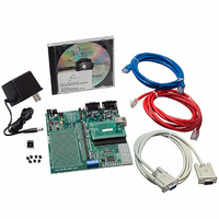
Manufacturer Part Number
NNDK-MOD5272-KIT
Description
KIT DEVELOP NETWORK FOR MOD5272
Manufacturer
NetBurner Inc
Series
ColdFire®r
Datasheets
1.MOD5272-100IR.pdf
(2 pages)
2.MOD5272-100IR.pdf
(550 pages)
3.NNDK-MOD5282-KIT.pdf
(2 pages)
Specifications of NNDK-MOD5272-KIT
Main Purpose
*
Embedded
*
Utilized Ic / Part
MOD5272
Primary Attributes
*
Secondary Attributes
*
Processor To Be Evaluated
MOD5272
Interface Type
RS-232, RS-485, USB
Lead Free Status / RoHS Status
Contains lead / RoHS non-compliant
Lead Free Status / RoHS Status
Lead free / RoHS Compliant, Contains lead / RoHS non-compliant
Other names
528-1001


AC Electrical Specifications
Read/write SRAM bus timings listed in Table 23-8 are shown in Figure 23-3, Figure 23-4,
Figure 23-5, and Figure 23-6.
1
2
23-8
B6a
B6b
B6c
B6d
B6e
B7a
B7b
B7c
B8
B9
B11
B12
B13
Name
All timing references to SDCLK are given to its rising edge when bit 3 of the SDRAM control register is 0.
Data output is held valid for one CPU clock period after deassertion of BS[3:0]
2
SDCLK to chip selects (CS[6:0]) valid
SDCLK to byte enables (BS[3:0]) valid
SDCLK to output enable (OE) valid
SDCLK to write enable (R/W) valid
SDCLK to reset output (RSTO) valid
SDCLK to control output (CS[6:0], OE) invalid (output hold)
SDCLK to control output (BS[3:0], R/W) invalid (output hold)
SDCLK to reset output (RSTO) invalid (output hold)
SDCLK to address (A[22:0]) valid
SDCLK to address (A[22:0]) invalid (output hold)
SDCLK to data output (D[31:0]) valid
SDCLK to data output (D[31:0]) invalid (output hold)
SDCLK to data output (D[31:0]) high impedance
Above 48 MHz, the memory bus may need to be configured for
one wait state. It is the responsibility of the user to determine
the actual frequency at which to insert a wait state since this
depends on the access time of SRAM or SDRAM used in a
particular system implementation.
Wait states are inserted for SRAM accesses by programming
bits 6–2 of the chip select option registers.
A wait state is added for SDRAM read accesses by setting bit
4 of the SDRAM control register.
Table 23-8. Processor Bus Output Timing Specifications
Characteristic
Address and Attribute Outputs
MCF5272 User’s Manual
Control Outputs
Data Outputs
NOTE:
1
Min
1.5
1.0
1.5
—
—
—
—
—
—
—
—
4
1
0–66 MHz
Max
13.5
13.0
9.5
9.0
12
11
—
—
—
—
—
8
6
MOTOROLA
Unit
nS
nS
nS
nS
nS
nS
nS
nS
nS
nS
nS
nS
nS
Related parts for NNDK-MOD5272-KIT
Image
Part Number
Description
Manufacturer
Datasheet
Request
R

Part Number:
Description:
BOARD SERIAL-ETHERNET 512K FLASH
Manufacturer:
NetBurner Inc
Datasheet:

Part Number:
Description:
PROCESSOR MODULE FLASH MOD5272
Manufacturer:
NetBurner Inc
Datasheet:

Part Number:
Description:
PROCESSOR MODULE 512KB FLASH
Manufacturer:
NetBurner Inc
Datasheet:

Part Number:
Description:
DUAL PORT SERIAL-ETHERNET
Manufacturer:
NetBurner Inc
Datasheet:

Part Number:
Description:
PROCESSOR MODULE FLASH
Manufacturer:
NetBurner Inc
Datasheet:

Part Number:
Description:
PROCESSOR MODULE 512KB FLASH
Manufacturer:
NetBurner Inc
Datasheet:

Part Number:
Description:
MOD5234 10/100 ETHERNET MODULE
Manufacturer:
NetBurner Inc
Datasheet:

Part Number:
Description:
KIT DEVELOP NETWORK FOR MOD5282
Manufacturer:
NetBurner Inc
Datasheet:

Part Number:
Description:
DUAL PORT SERIAL-ETHERNET
Manufacturer:
NetBurner Inc
Datasheet:

Part Number:
Description:
Ethernet Modules & Development Tools 32 Bit 66MHz 40 Pin DIP Industrial Temp
Manufacturer:
NetBurner Inc
Datasheet:

Part Number:
Description:
Ethernet Modules & Development Tools MOD5213 DEVELOPMENT KIT
Manufacturer:
NetBurner Inc

Part Number:
Description:
Ethernet Modules & Development Tools DUAL PORT SERIAL EHTERNET DEVICE
Manufacturer:
NetBurner Inc
Datasheet:

Part Number:
Description:
Ethernet ICs 32bit 147MHz CAN-to- Ethnt Device IndTemp
Manufacturer:
NetBurner Inc
Datasheet: