NNDK-MOD5272-KIT NetBurner Inc, NNDK-MOD5272-KIT Datasheet - Page 458
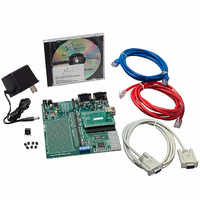
NNDK-MOD5272-KIT
Manufacturer Part Number
NNDK-MOD5272-KIT
Description
KIT DEVELOP NETWORK FOR MOD5272
Manufacturer
NetBurner Inc
Series
ColdFire®r
Datasheets
1.MOD5272-100IR.pdf
(2 pages)
2.MOD5272-100IR.pdf
(550 pages)
3.NNDK-MOD5282-KIT.pdf
(2 pages)
Specifications of NNDK-MOD5272-KIT
Main Purpose
*
Embedded
*
Utilized Ic / Part
MOD5272
Primary Attributes
*
Secondary Attributes
*
Processor To Be Evaluated
MOD5272
Interface Type
RS-232, RS-485, USB
Lead Free Status / RoHS Status
Contains lead / RoHS non-compliant
Lead Free Status / RoHS Status
Lead free / RoHS Compliant, Contains lead / RoHS non-compliant
Other names
528-1001


Bus Exception: Double Bus Fault
20.3 Bus Exception: Double Bus Fault
When a bus error or an address error occurs during the exception processing sequence for
a previous bus error, a previous address error, or a reset exception, the bus or address error
causes a double bus fault. If the MCF5272 experiences a double bus fault, it enters the
halted state. To exit the halt state, reset the MCF5272.
20.4 Bus Characteristics
The MCF5272 uses the address bus (A[22:0]) to specify the location for a data transfer and
the data bus (D[31:0] or D[31:16]) to transfer the data. Control signals indicate the direction
of the transfer. The selected device or the number of wait states programmed in the chip
select base registers (CSBRs), the chip select option registers (CSORs), the SDRAM
configuration and SDRAM timing registers (SDCR, SDTR) control the length of the cycle.
The MCF5272 clock is distributed internally to provide logic timing. All SRAM and ROM
mode bus signals should be considered as asynchronous with respect to CLKIN.
SDCR[INV] allows the SDRAM control signals to be asserted and negated synchronous
with the rising or falling edge of SDCLK. The SDRAM control signals are BS[3:0],
SDBA[1:0], RAS0, CAS0, SDWE, A10_PRECHG, SDCLKE, and CS7/SDCS.
The asynchronous INT[6:1] signals are internally synchronized to resolve the input to a
valid level before being used.
20.5 Data Transfer Mechanism
The MCF5272 supports byte, word, and longword operands and allows accesses to 8-, 16-,
and 32-bit data ports. The MCF5272 supports port sizes of the specific memory, enables
internal generation of transfer termination, and sets the number of wait states for the
external slave being accessed by programming the CSBRs, CSORs, SDCR, and SDTR. For
more information on programming these registers, refer to the SIM, chip select, and
SDRAM controller chapters.
20-4
Table 20-2. Chip Select Memory Address Decoding Priority
The MCF5272 compares the address for the current bus
transfer with the address and mask bits in the CSBRs and
CSORs looking for a match. The priority is listed in Table 20-2
(from highest priority to lowest priority):
Priority
Highest
MCF5272 User’s Manual
NOTE:
Chip Select 0
Chip Select 1
Chip Select 2
Chip Select
MOTOROLA
Related parts for NNDK-MOD5272-KIT
Image
Part Number
Description
Manufacturer
Datasheet
Request
R

Part Number:
Description:
BOARD SERIAL-ETHERNET 512K FLASH
Manufacturer:
NetBurner Inc
Datasheet:

Part Number:
Description:
PROCESSOR MODULE FLASH MOD5272
Manufacturer:
NetBurner Inc
Datasheet:

Part Number:
Description:
PROCESSOR MODULE 512KB FLASH
Manufacturer:
NetBurner Inc
Datasheet:

Part Number:
Description:
DUAL PORT SERIAL-ETHERNET
Manufacturer:
NetBurner Inc
Datasheet:

Part Number:
Description:
PROCESSOR MODULE FLASH
Manufacturer:
NetBurner Inc
Datasheet:

Part Number:
Description:
PROCESSOR MODULE 512KB FLASH
Manufacturer:
NetBurner Inc
Datasheet:

Part Number:
Description:
MOD5234 10/100 ETHERNET MODULE
Manufacturer:
NetBurner Inc
Datasheet:

Part Number:
Description:
KIT DEVELOP NETWORK FOR MOD5282
Manufacturer:
NetBurner Inc
Datasheet:

Part Number:
Description:
DUAL PORT SERIAL-ETHERNET
Manufacturer:
NetBurner Inc
Datasheet:

Part Number:
Description:
Ethernet Modules & Development Tools 32 Bit 66MHz 40 Pin DIP Industrial Temp
Manufacturer:
NetBurner Inc
Datasheet:

Part Number:
Description:
Ethernet Modules & Development Tools MOD5213 DEVELOPMENT KIT
Manufacturer:
NetBurner Inc

Part Number:
Description:
Ethernet Modules & Development Tools DUAL PORT SERIAL EHTERNET DEVICE
Manufacturer:
NetBurner Inc
Datasheet:

Part Number:
Description:
Ethernet ICs 32bit 147MHz CAN-to- Ethnt Device IndTemp
Manufacturer:
NetBurner Inc
Datasheet: