NNDK-MOD5272-KIT NetBurner Inc, NNDK-MOD5272-KIT Datasheet - Page 490
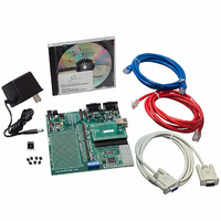
NNDK-MOD5272-KIT
Manufacturer Part Number
NNDK-MOD5272-KIT
Description
KIT DEVELOP NETWORK FOR MOD5272
Manufacturer
NetBurner Inc
Series
ColdFire®r
Datasheets
1.MOD5272-100IR.pdf
(2 pages)
2.MOD5272-100IR.pdf
(550 pages)
3.NNDK-MOD5282-KIT.pdf
(2 pages)
Specifications of NNDK-MOD5272-KIT
Main Purpose
*
Embedded
*
Utilized Ic / Part
MOD5272
Primary Attributes
*
Secondary Attributes
*
Processor To Be Evaluated
MOD5272
Interface Type
RS-232, RS-485, USB
Lead Free Status / RoHS Status
Contains lead / RoHS non-compliant
Lead Free Status / RoHS Status
Lead free / RoHS Compliant, Contains lead / RoHS non-compliant
Other names
528-1001


Restrictions
Figure 21-8 shows the structure of the bypass register.
21.6 Restrictions
The control afforded by the output enable signals using the boundary scan register and the
EXTEST instruction requires a compatible circuit board test environment to avoid
configurations that could damage the device. The user must avoid situations in which the
MCF5272 output drivers are enabled into actively driven networks. Overdriving the TDO
driver when it is active is not recommended.
21-8
B[3:0] Instruction
0010
1001
1100
1101
1111
PRELOAD
SAMPLE/
Reserved
BYPASS
CLAMP
HI-Z
The SAMPLE/PRELOAD instruction selects the boundary scan register and provides two
separate functions. First, it provides a means to obtain a snapshot of system data and
control signals. The snapshot occurs on the rising edge of TCK in the capture-DR controller
state. The data can be observed by shifting it transparently through the boundary scan
register.
Because there is no internal synchronization between the IEEE 1149.1 clock (TCK) and the
system clock (CLKOUT), the user must provide some form of external synchronization to
achieve meaningful results.
The second function of SAMPLE/PRELOAD is to initialize the boundary scan register output
bits prior to selection of EXTEST. This initialization ensures that known data appears on the
outputs when entering the EXTEST instruction.
The HI-Z instruction anticipates the need to backdrive the output pins and protect the input
pins from random toggling during circuit board testing. The HIGHZ instruction selects the
bypass register, forcing all output and bidirectional pins to the high-impedance state.
The HI-Z instruction goes active on the falling edge of TCK in the update-IR state when the
data held in the instruction shift register is equivalent to octal 5.
When the CLAMP instruction is invoked, the boundary scan multiplexer control signal
EXTEST is asserted, and the BYPASS register is selected. CLAMP should be invoked after
valid data has been shifted into the boundary scan register, e.g., by SAMPLE/PRELOAD.
CLAMP allows static levels to be presented at the MCF5272 output and bidirectional pins,
like EXTEST, but without the shift latency of the boundary scan register from TDI to TDO.
Reserved
The BYPASS instruction selects the single-bit bypass register as shown in Figure 21-8. This
creates a shift register path from TDI to the bypass register and, finally, to TDO,
circumventing the boundary scan register. This instruction is used to enhance test efficiency
when a component other than the MCF5272 becomes the device under test. When the
bypass register is selected by the current instruction, the shift register stage is set to a logic
zero on the rising edge of TCK in the capture-DR controller state. Therefore, the first bit to be
shifted out after selecting the bypass register is always a logic zero.
FROM TDI
SHIFT DR
Table 21-2. Instructions (Continued)
0
Figure 21-8. Bypass Register
MCF5272MCF5272 User’s Manual
G1
1
1
MUX
CLOCK DR
Description
1 D
C1
TO TDO
MOTOROLA
Related parts for NNDK-MOD5272-KIT
Image
Part Number
Description
Manufacturer
Datasheet
Request
R

Part Number:
Description:
BOARD SERIAL-ETHERNET 512K FLASH
Manufacturer:
NetBurner Inc
Datasheet:

Part Number:
Description:
PROCESSOR MODULE FLASH MOD5272
Manufacturer:
NetBurner Inc
Datasheet:

Part Number:
Description:
PROCESSOR MODULE 512KB FLASH
Manufacturer:
NetBurner Inc
Datasheet:

Part Number:
Description:
DUAL PORT SERIAL-ETHERNET
Manufacturer:
NetBurner Inc
Datasheet:

Part Number:
Description:
PROCESSOR MODULE FLASH
Manufacturer:
NetBurner Inc
Datasheet:

Part Number:
Description:
PROCESSOR MODULE 512KB FLASH
Manufacturer:
NetBurner Inc
Datasheet:

Part Number:
Description:
MOD5234 10/100 ETHERNET MODULE
Manufacturer:
NetBurner Inc
Datasheet:

Part Number:
Description:
KIT DEVELOP NETWORK FOR MOD5282
Manufacturer:
NetBurner Inc
Datasheet:

Part Number:
Description:
DUAL PORT SERIAL-ETHERNET
Manufacturer:
NetBurner Inc
Datasheet:

Part Number:
Description:
Ethernet Modules & Development Tools 32 Bit 66MHz 40 Pin DIP Industrial Temp
Manufacturer:
NetBurner Inc
Datasheet:

Part Number:
Description:
Ethernet Modules & Development Tools MOD5213 DEVELOPMENT KIT
Manufacturer:
NetBurner Inc

Part Number:
Description:
Ethernet Modules & Development Tools DUAL PORT SERIAL EHTERNET DEVICE
Manufacturer:
NetBurner Inc
Datasheet:

Part Number:
Description:
Ethernet ICs 32bit 147MHz CAN-to- Ethnt Device IndTemp
Manufacturer:
NetBurner Inc
Datasheet: