NNDK-MOD5272-KIT NetBurner Inc, NNDK-MOD5272-KIT Datasheet - Page 432
NNDK-MOD5272-KIT
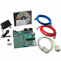
Manufacturer Part Number
NNDK-MOD5272-KIT
Description
KIT DEVELOP NETWORK FOR MOD5272
Manufacturer
NetBurner Inc
Series
ColdFire®r
Datasheets
1.MOD5272-100IR.pdf
(2 pages)
2.MOD5272-100IR.pdf
(550 pages)
3.NNDK-MOD5282-KIT.pdf
(2 pages)
Specifications of NNDK-MOD5272-KIT
Main Purpose
*
Embedded
*
Utilized Ic / Part
MOD5272
Primary Attributes
*
Secondary Attributes
*
Processor To Be Evaluated
MOD5272
Interface Type
RS-232, RS-485, USB
Lead Free Status / RoHS Status
Contains lead / RoHS non-compliant
Lead Free Status / RoHS Status
Lead free / RoHS Compliant, Contains lead / RoHS non-compliant
Other names
528-1001


Address Bus (A[22:0]/SDA[13:0])
19.3 Address Bus (A[22:0]/SDA[13:0])
The 23 dedicated address signals, A[22:0], define the address of external byte, word, and
longword accesses. These three-state outputs are the 23 lsbs of the internal 32-bit address
bus and are multiplexed with the SDRAM controller row and column addresses
(SDA[13:0]).
Fourteen address signals are used for connecting to SDRAM devices as large as 256 Mbits.
The MCF5272 supports SDRAM widths of 16 or 32 bits. For a 32-bit width, SDRAM
address signals are multiplexed starting with A2. For a 16-bit width, address signals are
multiplexed starting with A1.
19.4 Data Bus (D[31:0])
The 32-bit, three-state, bidirectional, non-multiplexed data bus transfers data to and from
the MCF5272. A read or write operation can transfer 8, 16, or 32 bits in one bus cycle.
When a 16-bit data bus is used, mode parallel port C pins can be multiplexed onto D[15:0].
Data read from or written to on-chip peripherals is visible on the external data bus when the
device’s external bus width is 32 bits. When the device is configured for external 16-bit
wide data bus and the data access is 32 bits wide, the lower 16 bits of on-chip data are not
visible externally. On-chip cache, ROM, and SRAM accesses are not visible externally.
19.4.1 Dynamic Data Bus Sizing
When the device is in normal mode, dynamic bus sizing lets the programmer change data
bus width between 8, 32, and 16 bits for each chip select. The initial width for the bootstrap
program chip select, CS0, is determined by the state of BUSW[1:0]. The program should
select bus widths for the other chip selects before accessing the associated memory space.
BGA
Map
19-18
P10
P11
P12
P13
P14
Pin
P9
Table 19-2. Signal Name and Description by Pin Number (Continued)
0 (Reset)
OE/RD
PB11
PB15
CS2
CS6
R/W
Pin Functions
E_RxD3
E_MDC
1
–
–
–
–
MCF5272 User’s Manual
2
–
–
–
–
–
–
3
–
–
–
–
–
–
PB11/E_RxD3
PB15/E_MDC
CS6/AEN
OE/RD
Name
CS2
R/W
Port B bit 11/Rx data bit
3 (100 Base-T Ethernet
only)
Port B bit 15/
Management Channel
Clock (100 Base-T only)
Chip select 2
Chip select 6
Output enable/Read
Read/Write
Description
MOTOROLA
I/O
I/O
I/O
O
O
O
O
Related parts for NNDK-MOD5272-KIT
Image
Part Number
Description
Manufacturer
Datasheet
Request
R

Part Number:
Description:
BOARD SERIAL-ETHERNET 512K FLASH
Manufacturer:
NetBurner Inc
Datasheet:

Part Number:
Description:
PROCESSOR MODULE FLASH MOD5272
Manufacturer:
NetBurner Inc
Datasheet:

Part Number:
Description:
PROCESSOR MODULE 512KB FLASH
Manufacturer:
NetBurner Inc
Datasheet:

Part Number:
Description:
DUAL PORT SERIAL-ETHERNET
Manufacturer:
NetBurner Inc
Datasheet:

Part Number:
Description:
PROCESSOR MODULE FLASH
Manufacturer:
NetBurner Inc
Datasheet:

Part Number:
Description:
PROCESSOR MODULE 512KB FLASH
Manufacturer:
NetBurner Inc
Datasheet:

Part Number:
Description:
MOD5234 10/100 ETHERNET MODULE
Manufacturer:
NetBurner Inc
Datasheet:

Part Number:
Description:
KIT DEVELOP NETWORK FOR MOD5282
Manufacturer:
NetBurner Inc
Datasheet:

Part Number:
Description:
DUAL PORT SERIAL-ETHERNET
Manufacturer:
NetBurner Inc
Datasheet:

Part Number:
Description:
Ethernet Modules & Development Tools 32 Bit 66MHz 40 Pin DIP Industrial Temp
Manufacturer:
NetBurner Inc
Datasheet:

Part Number:
Description:
Ethernet Modules & Development Tools MOD5213 DEVELOPMENT KIT
Manufacturer:
NetBurner Inc

Part Number:
Description:
Ethernet Modules & Development Tools DUAL PORT SERIAL EHTERNET DEVICE
Manufacturer:
NetBurner Inc
Datasheet:

Part Number:
Description:
Ethernet ICs 32bit 147MHz CAN-to- Ethnt Device IndTemp
Manufacturer:
NetBurner Inc
Datasheet: