NNDK-MOD5272-KIT NetBurner Inc, NNDK-MOD5272-KIT Datasheet - Page 344
NNDK-MOD5272-KIT
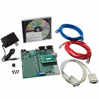
Manufacturer Part Number
NNDK-MOD5272-KIT
Description
KIT DEVELOP NETWORK FOR MOD5272
Manufacturer
NetBurner Inc
Series
ColdFire®r
Datasheets
1.MOD5272-100IR.pdf
(2 pages)
2.MOD5272-100IR.pdf
(550 pages)
3.NNDK-MOD5282-KIT.pdf
(2 pages)
Specifications of NNDK-MOD5272-KIT
Main Purpose
*
Embedded
*
Utilized Ic / Part
MOD5272
Primary Attributes
*
Secondary Attributes
*
Processor To Be Evaluated
MOD5272
Interface Type
RS-232, RS-485, USB
Lead Free Status / RoHS Status
Contains lead / RoHS non-compliant
Lead Free Status / RoHS Status
Lead free / RoHS Compliant, Contains lead / RoHS non-compliant
Other names
528-1001


Operation
14.4.1.2 Transmit RAM
Data to be transmitted by the QSPI is stored in the transmit RAM segment located at
addresses 0x0 to 0xF. The user normally writes 1 word into this segment for each queue
command to be executed. The user cannot read transmit RAM.
Out-bound data must be written to transmit RAM in a right-justified format. The unused
bits are ignored. The QSPI copies the data to its data serializer (shift register) for
transmission. The data is transmitted most significant bit first and remains in transmit RAM
until overwritten by the user.
14.4.1.3 Command RAM
The CPU writes one byte of control information to this segment for each QSPI command
to be executed. Command RAM is write-only memory from a user’s perspective.
Command RAM consists of 16 bytes with each byte divided into two fields. The peripheral
chip select field controls the QSPI_CS signal levels for the transfer. The command control
field provides transfer options.
A maximum of 16 commands can be in the queue. Queue execution proceeds from the
address in QWR[NEWQP] through the address in QWR[ENDQP].
The QSPI executes a queue of commands defined by the control bits in each command
RAM entry which sequence the following actions:
Before any data transfers begin, control data must be written to the command RAM, and
any out-bound data must be written to transmit RAM. Also, the queue pointers must be
initialized to the first and last entries in the command queue.
Data transfer is synchronized with the internally generated QSPI_CLK, whose phase and
polarity are controlled by QMR[CPHA] and QMR[CPOL]. These control bits determine
which QSPI_CLK edge is used to drive outgoing data and to latch incoming data.
14.4.2 Baud Rate Selection
The maximum QSPI clock frequency is one-fourth the clock frequency applied at the
CLKIN pin. Baud rate is selected by writing a value from 2–255 into QMR[BAUD]. The
QSPI uses a prescaler to derive the QSPI_CLK rate from the system clock, CLKIN, divided
by two.
A baud rate value of zero turns off the QSPI_CLK. The desired QSPI_CLK baud rate is
related to CLKIN and QMR[BAUD] by the following expression:
14-6
• chip-select pins are activated
• data is transmitted from transmit RAM and received into the receive RAM
• the synchronous transfer clock QSPI_CLK is generated
QMR[BAUD] = CLKIN / [2 × (desired QSPI_CLK baud rate)]
MCF5272 User’s Manual
MOTOROLA
Related parts for NNDK-MOD5272-KIT
Image
Part Number
Description
Manufacturer
Datasheet
Request
R

Part Number:
Description:
BOARD SERIAL-ETHERNET 512K FLASH
Manufacturer:
NetBurner Inc
Datasheet:

Part Number:
Description:
PROCESSOR MODULE FLASH MOD5272
Manufacturer:
NetBurner Inc
Datasheet:

Part Number:
Description:
PROCESSOR MODULE 512KB FLASH
Manufacturer:
NetBurner Inc
Datasheet:

Part Number:
Description:
DUAL PORT SERIAL-ETHERNET
Manufacturer:
NetBurner Inc
Datasheet:

Part Number:
Description:
PROCESSOR MODULE FLASH
Manufacturer:
NetBurner Inc
Datasheet:

Part Number:
Description:
PROCESSOR MODULE 512KB FLASH
Manufacturer:
NetBurner Inc
Datasheet:

Part Number:
Description:
MOD5234 10/100 ETHERNET MODULE
Manufacturer:
NetBurner Inc
Datasheet:

Part Number:
Description:
KIT DEVELOP NETWORK FOR MOD5282
Manufacturer:
NetBurner Inc
Datasheet:

Part Number:
Description:
DUAL PORT SERIAL-ETHERNET
Manufacturer:
NetBurner Inc
Datasheet:

Part Number:
Description:
Ethernet Modules & Development Tools 32 Bit 66MHz 40 Pin DIP Industrial Temp
Manufacturer:
NetBurner Inc
Datasheet:

Part Number:
Description:
Ethernet Modules & Development Tools MOD5213 DEVELOPMENT KIT
Manufacturer:
NetBurner Inc

Part Number:
Description:
Ethernet Modules & Development Tools DUAL PORT SERIAL EHTERNET DEVICE
Manufacturer:
NetBurner Inc
Datasheet:

Part Number:
Description:
Ethernet ICs 32bit 147MHz CAN-to- Ethnt Device IndTemp
Manufacturer:
NetBurner Inc
Datasheet: